Modulation circuit and semiconductor device including the same
a technology of modulation circuit and semiconductor device, which is applied in the direction of modulation, semiconductor/solid-state device details, instruments, etc., can solve the problems of reducing the reliability of rfid communication and increasing power consumption, so as to reduce the power consumption of the modulation circuit, and reduce the power consumption
- Summary
- Abstract
- Description
- Claims
- Application Information
AI Technical Summary
Benefits of technology
Problems solved by technology
Method used
Image
Examples
embodiment 1
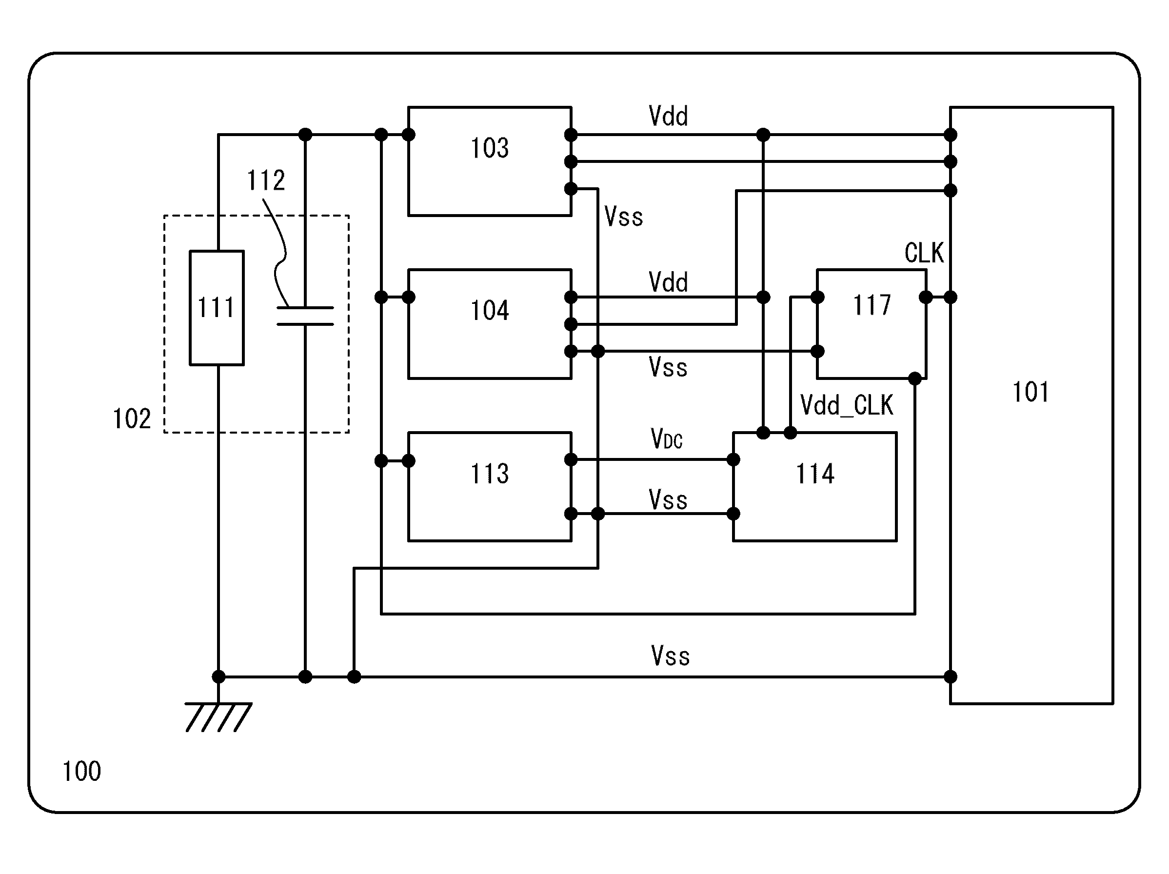
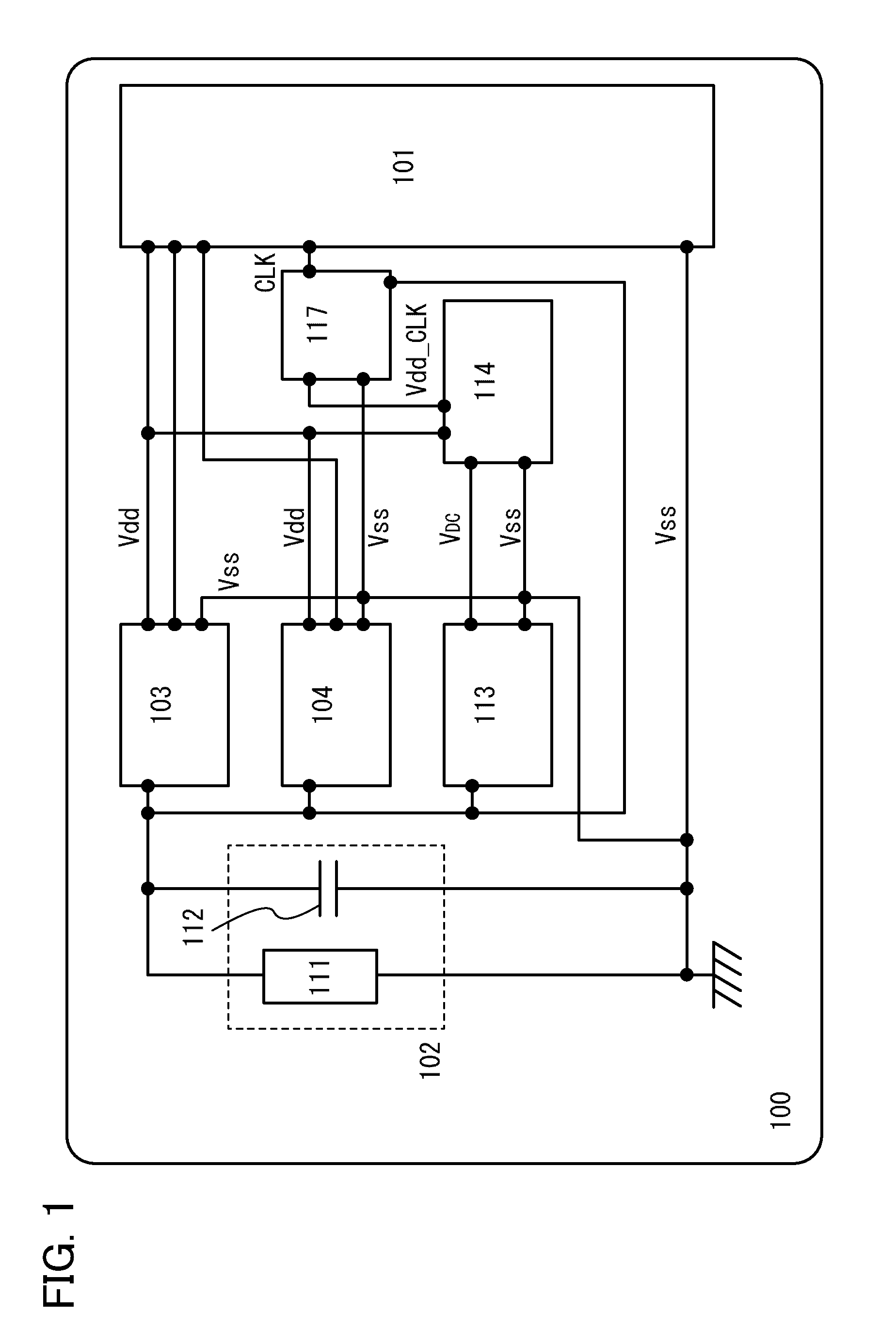
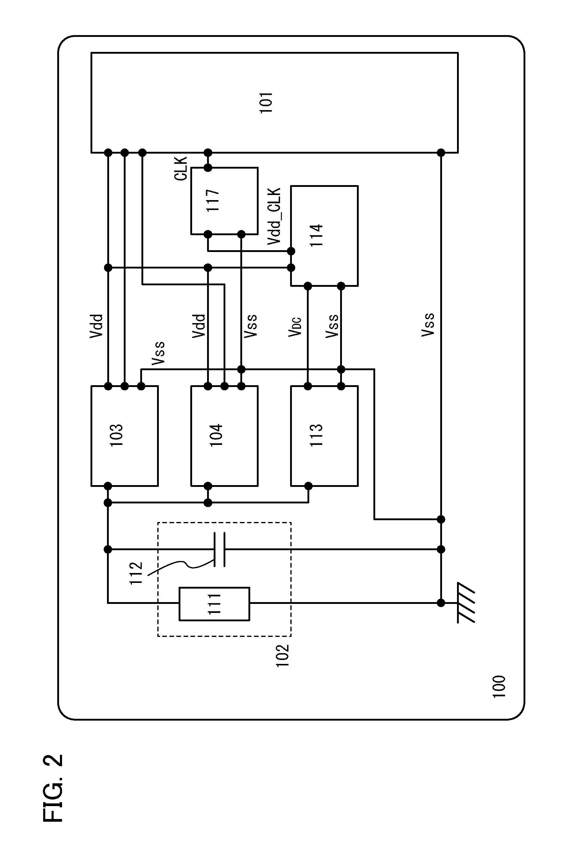
[0051]FIG. 1 shows the block diagram of the whole RF tag which is used as one embodiment of the present invention. An RF tag 100 include: a logic circuit 101 which carries out functional processing, e.g. generates a response signal in response to data received; an antenna circuit 102 which sends and receives signals to / from (communicates with) a reader / writer; a demodulation circuit 103 which demodulates an amplitude-modulated wave (obtained by superimposing a modulated wave on a carrier wave) received by the antenna circuit 102 to extract a pulsed signal; a modulation circuit 104 which modulates a carrier wave outputted from the reader / writer in response to a response signal outputted from the logic circuit 101 and transmitting a response signal to the reader / writer; a rectifier circuit 113 for generating a DC voltage from a carrier wave or amplitude-modulated wave received by the antenna circuit 102; a constant-voltage circuit 114 which converts DC voltage generated by the rectifi...
embodiment 2
[0060]In this embodiment, the configuration of the modulation circuit described in Embodiment 1 will be described.
[0061]FIG. 3 shows an example of the circuit configuration of the modulation circuit according to one embodiment of the present invention. A modulation circuit 301 employs a load modulation method, and includes a load 302 and a transistor 303. One of the source and drain of the transistor 303 is electrically connected to one terminal of an antenna 304 through the load 302. The other of the source and drain is electrically connected to the other terminal of the antenna 304. The on / off of the transistor 303 is controlled in accordance with a signal 305 inputted to the gate of the transistor 303. Note that the signal 305 inputted to the gate of the transistor 303 is a binary signal with high (H) or low (L), and corresponds to a response signal outputted from the logic circuit (also referred to as a subcarrier).
[0062]In this manner, the modulation circuit 301 using a load mo...
embodiment 3
[0105]In this embodiment, a configuration whereby the power consumption of the modulation circuit is further reduced will be described.
[0106]First, one example of the configuration of the modulation circuit of this embodiment will be described with reference to FIG. 7. FIG. 7 is different from FIG. 3 described in Embodiment 1 in that a modulation circuit 701 shown in FIG. 7 has a load 702, a transistor 703, and a diode 720 which are connected in series between the two terminals of the antenna 304, while the modulation circuit 301 shown in FIG. 3 has the load 302 and the transistor 303 are connected in series between the two terminals of the antenna 304. In other words, the modulation circuit 701 shown in FIG. 7 includes the load 702, the transistor 703, and the diode 720. One terminal of the load 702 is electrically connected to one terminal of the antenna 304, and the other terminal of the load 702 is electrically connected to the anode (one terminal) of the diode 720. The cathode ...
PUM
 Abstract
Description
Claims
Application Information


