Interlayer insulating film, wiring structure, and methods of manufacturing the same

Inactive Publication Date: 2011-06-02
TOHOKU UNIV +3
View PDF6 Cites 4 Cited by
  • Summary
  • Abstract
  • Description
  • Claims
  • Application Information

AI Technical Summary

Benefits of technology

[0040]According to this invention, since an interlayer insulating film is formed by coating a liquid coating film and then drying it

Problems solved by technology

In a semiconductor device employing such a multilayer wiring structure, a problem of signal delay due to the parasitic capacitance between wirings

Method used


Image

  • Interlayer insulating film, wiring structure, and methods of manufacturing the same
  • Interlayer insulating film, wiring structure, and methods of manufacturing the same
  • Interlayer insulating film, wiring structure, and methods of manufacturing the same

Examples


Embodiment Construction

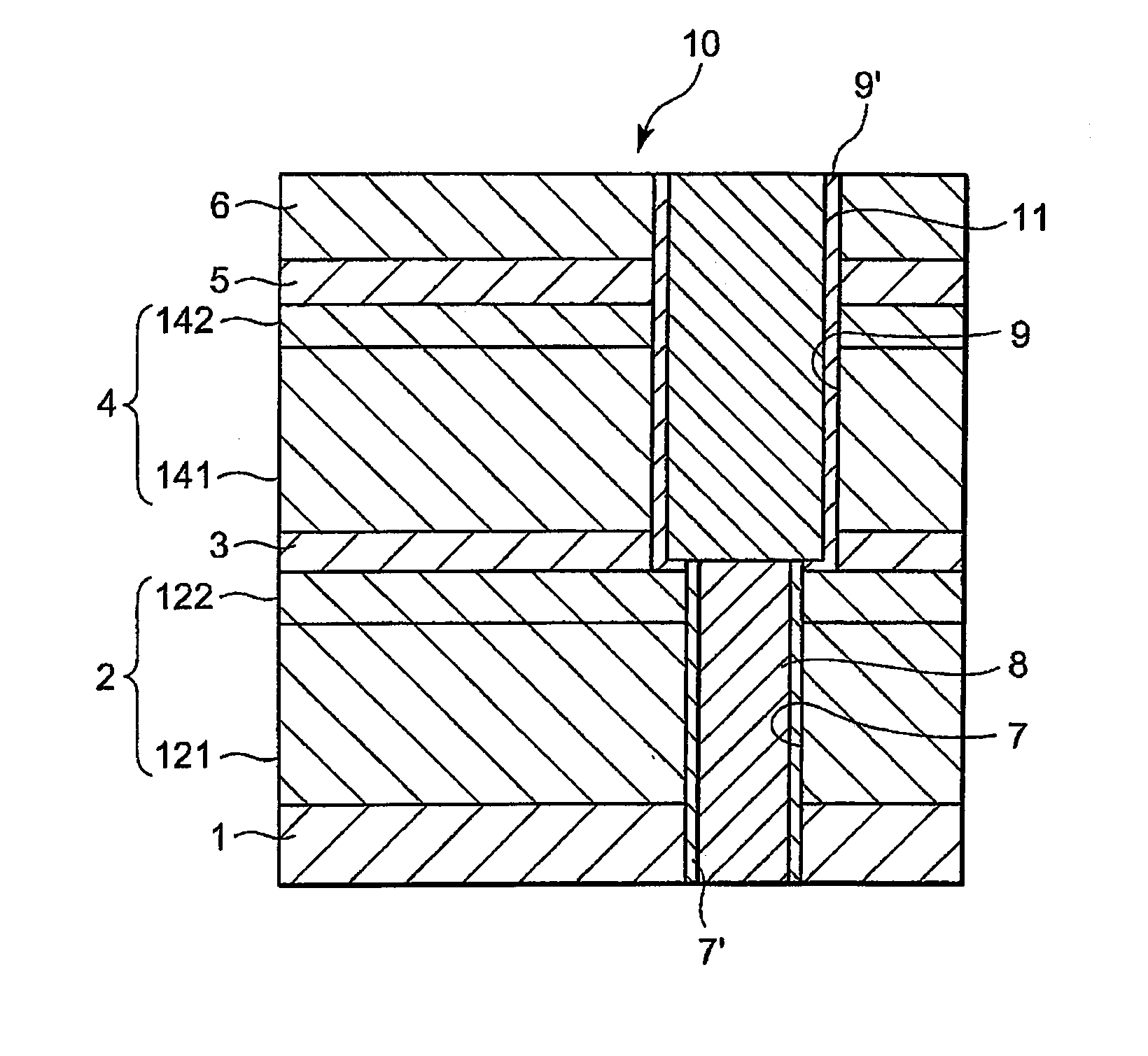
[0080]Hereinbelow, embodiments of this invention will be described with reference to the drawings.

[0081]FIG. 1 is a sectional view showing a wiring structure according to one embodiment of this invention. A semiconductor device shown in FIG. 1 has a multilayer wiring structure (only one connecting portion between wiring layers is shown) 10 provided over a semiconductor substrate (not shown) formed with a number of semiconductor elements. The illustrated multilayer wiring structure 10 is provided on a barrier cap layer 1 made of silicon carbonitride (SiCN) and provided on the semiconductor substrate and includes first and second interlayer insulating films 2 and 4, wherein these interlayer insulating films 2 and 4 insulate wiring layers and / or conductive regions formed in multilayers from each other.

[0082]The first interlayer insulating film 2 is provided with a via hole 7 penetrating the first interlayer insulating film 2 and the barrier cap layer 1. An electrode or wiring 8 made of...


PUM

PropertyMeasurementUnit
Temperatureaaaaaaaaaa
Thicknessaaaaaaaaaa
Nanoscale particle sizeaaaaaaaaaa

Abstract

An insulative coat film comprising one or two or more kinds of oxides having a dielectric constant (k) of 2.5 or smaller and expressed by a general formula of ((CH3)nSiO2-n/2)x(SiO2)1-x (where n=1 to 3, x≦1) is used to form an interlayer insulation film. The insulative coat film applied by spin-coating is flat without reflecting underlying unevenness, and the heat-treated film has surface roughness of 1 nm or less in Ra and 20 nm or less in a P-V value. The interlayer insulation film containing the insulative coat film can have a wiring structure and an electrode formed only by etching without need of a CMP process.

Description

TECHNICAL FIELD[0001]This invention relates to a multilayer wiring structure, particularly an interlayer insulating film structure, of a board such as a semiconductor element or semiconductor chip mounting board or a wiring board and further relates to a semiconductor device having the multilayer wiring structure, a wiring board having the multilayer wiring structure, and an electronic device including them. Moreover, this invention relates to a method of manufacturing the multilayer wiring structure and methods of manufacturing the semiconductor device having the multilayer wiring structure, the wiring board having the multilayer wiring structure, and the electronic device including them.BACKGROUND ART[0002]Conventionally, an interlayer insulating film is formed for insulation between wiring layers in a multilayer wiring structure on a semiconductor substrate or the like.[0003]In a semiconductor device employing such a multilayer wiring structure, a problem of signal delay due to t...

Claims


Application Information

Patent Timeline
IPC IPC(8): H05K1/11H05K3/46H05K3/36H05K1/00
CPCH01L21/0212H01L21/02126H01L2924/0002H01L21/022H01L21/02274H01L21/02304H01L21/02362H01L21/3121H01L21/316H01L21/76807H01L21/76819H01L21/76829H01L21/76832H01L21/76835H01L21/7684H01L21/76897H01L23/53238H01L23/5329H01L23/53295H01L2924/00
Inventor OHMI, TADAHIROMATSUOKA, TAKAAKIINOKUCHI, ATSUTOSHIWATANUKI, KOHEIKOIKE, TADASHIADACHI, TATSUHIKO
Owner TOHOKU UNIV
Why Eureka
Try Eureka