Manufacturing method of semiconductor integrated circuit device

a manufacturing method and integrated circuit technology, applied in solid-state devices, vacuum evaporation coatings, coatings, etc., can solve problems such as wiring failures and foreign materials or particles, and achieve the effect of reducing foreign materials

Inactive Publication Date: 2011-06-02
RENESAS ELECTRONICS CORP
View PDF4 Cites 15 Cited by
  • Summary
  • Abstract
  • Description
  • Claims
  • Application Information

AI Technical Summary

Benefits of technology

[0019]That is, in a case where the tantalum nitride film and the tantalum film are repeatedly deposited over each of a number of wafers in the sputtering deposition chamber, the manufacturing method of the semiconductor integrated circuit device includes the step of depositing over the substantial inner wall of the chamber the tantalum film for preventing foreign materia...

Problems solved by technology

Thus, when the thickness of the deposited film in the wet process (total thickness of the deposited film in the wet process) is large, the deposited film m...

Method used


Image

  • Manufacturing method of semiconductor integrated circuit device
  • Manufacturing method of semiconductor integrated circuit device
  • Manufacturing method of semiconductor integrated circuit device

Examples


Embodiment Construction

Outline of Preferred Embodiments

[0040]First, the outline of representative preferred embodiments of the invention disclosed in the present application will be described below.

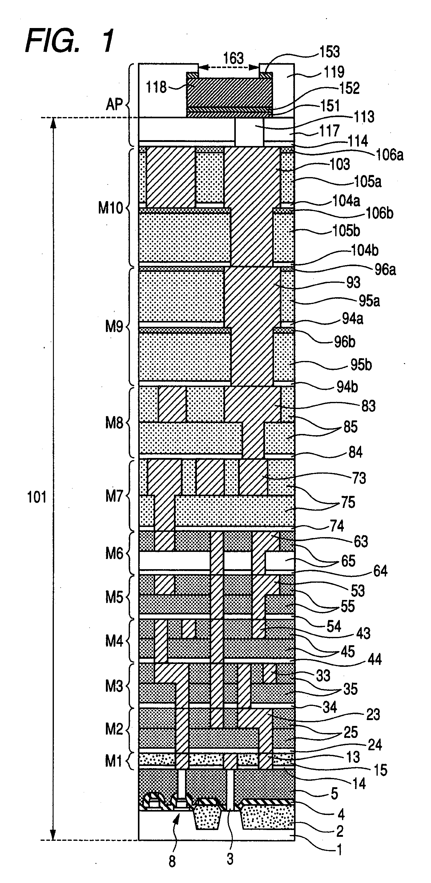
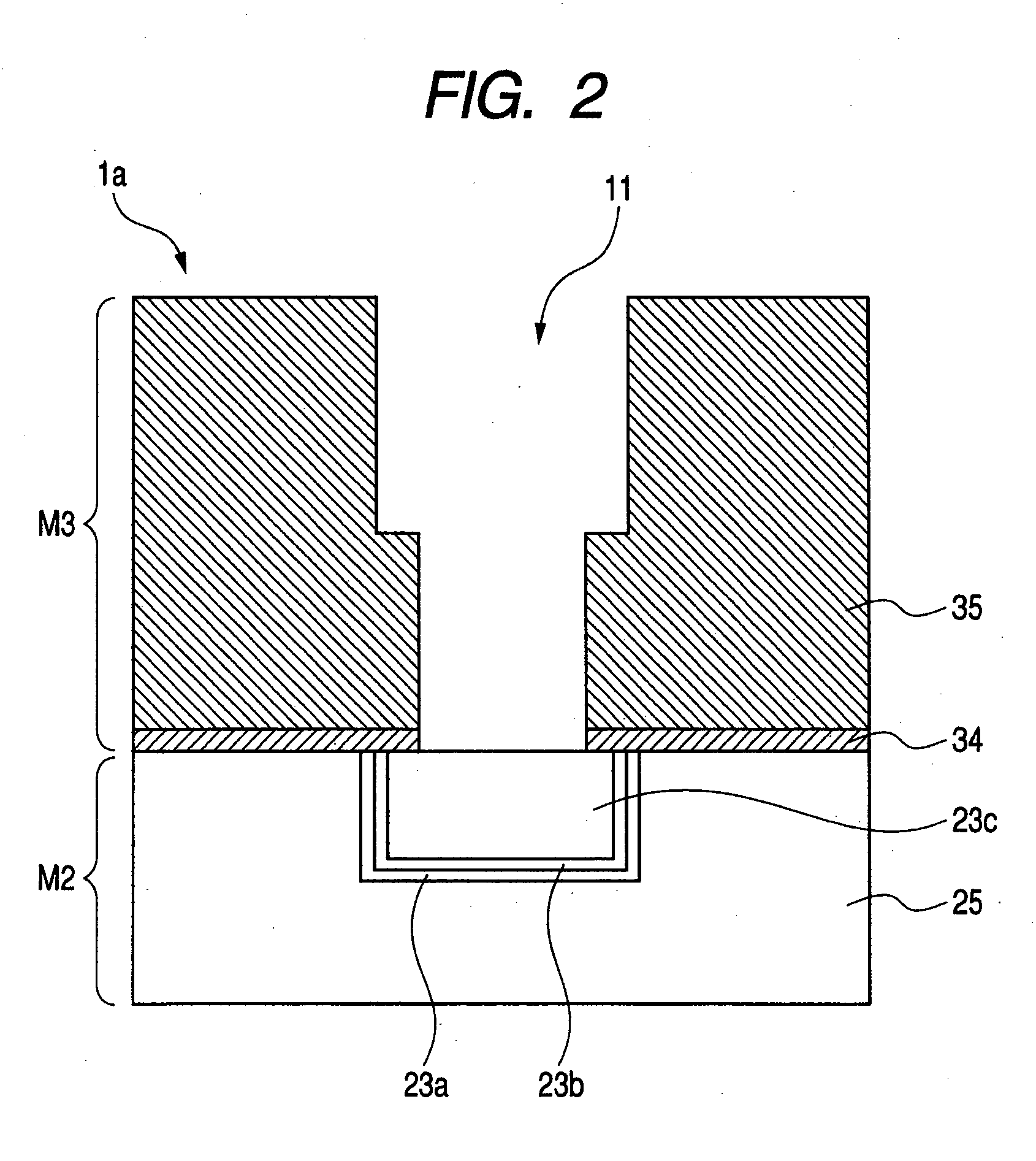
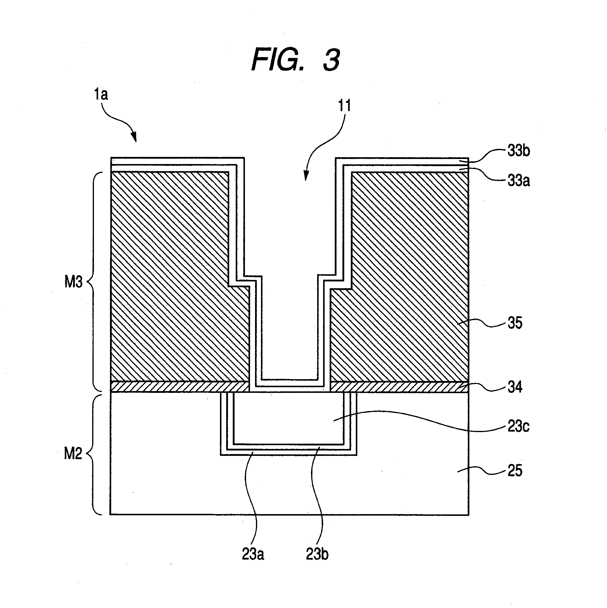
[0041]1. A manufacturing method of a semiconductor integrated circuit device includes the following steps of: (a) introducing a wafer to be processed, into a chamber; (b) depositing a tantalum nitride film having a first thickness over the wafer to be processed in the chamber by sputtering; (c) after the step (b), depositing a first tantalum film having a second thickness over the wafer to be processed in the chamber by the sputtering; (d) discharging the wafer to be processed to an outside of the chamber; (e) sequentially applying a lower-level process cycle including the steps (a) to (d) to a plurality of wafers to be processed that are different from the wafer belonging to a previous lower-level process cycle; (f) after the step (e), depositing a second tantalum film having a third thickness much larger than...


PUM

PropertyMeasurementUnit
Thicknessaaaaaaaaaa
Thicknessaaaaaaaaaa
Thicknessaaaaaaaaaa

Abstract

In a copper damascene wiring process, a tantalum-based laminated film, which is used as a barrier metal film, is continuously formed in a sputtering deposition chamber. When the continuous deposition process is discontinuously applied to a number of wafers, a tantalum film and a tantalum nitride film which are relatively thin are alternately deposited over an inner surface of a shield in a sputter deposition chamber, which results in a thickness of the deposited film being on the order of several thousand nanometers. The deposited film peels off due to internal stress therein to generate foreign material or particles. To counteract this, a tantalum film, which is much thicker than the tantalum film formed over the wafer at one time, is formed over the substantially inner wall of the chamber at predetermined intervals when repeatedly depositing the tantalum nitride film and the tantalum film in the sputtering deposition chamber.

Description

CROSS-REFERENCE TO RELATED APPLICATIONS[0001]The disclosure of Japanese Patent Application No. 2009-273240 filed on Dec. 1, 2009 including the specification, drawings and abstract is incorporated herein by reference in its entirety.BACKGROUND OF THE INVENTION[0002]The present invention relates to a technique effectively applied to metal sputtering deposition technology in a manufacturing method of a semiconductor integrated circuit device (or semiconductor device).[0003]Japanese Unexamined Patent Publication Number No. Hei 11(1999)-269644 (Patent Document 1) discloses a technique of sputter etching for removing a natural oxide film or the like in a different chamber before deposition of a metal film or the like by sputtering. In the technique, a film or the like of metal with a small stress, such as aluminum, is previously formed over an inner wall of the different chamber to suppress falling of particles of silicon oxide-based material.[0004]Japanese Unexamined Patent Publication N...

Claims


Application Information

Patent Timeline
IPC IPC(8): C23C14/34
CPCC23C14/564H01L21/2855H01L21/76805H01L21/76814H01L21/76843H01L21/76844H01L2224/02166H01L2924/1306H01L2924/13091H01L24/05H01L2924/00H01L2924/15788H01L2924/14
Inventor HAMAYA, TAKASHISUZUKI, HIDENORIHARANO, YUICHIITO, MASAHIKO
Owner RENESAS ELECTRONICS CORP
Why Eureka
Try Eureka