Semiconductor device and manufacturing method thereof

a technology of semiconductors and semiconductors, applied in the direction of semiconductor devices, electrical devices, transistors, etc., can solve the problems of insufficient characteristics in fact, and achieve the effect of excellent electrical characteristics

Active Publication Date: 2011-06-09
SEMICON ENERGY LAB CO LTD
View PDF100 Cites 118 Cited by
  • Summary
  • Abstract
  • Description
  • Claims
  • Application Information

AI Technical Summary

Benefits of technology

[0034]Electrical characteristics are different between an oxide semiconductor layer including a crystalline region having electrical anisotropy and an oxide semiconductor layer without a crystalline region. For example, in an oxide semiconductor layer including a crystalline region having c-axis aligned in a direction substantially perpendicular to a surface of the oxide semiconductor layer, conductivity in a direction parallel to the surface of the oxide semiconductor layer is increased and an insulating property in a direction perpendicular to the surface of the oxide semiconductor layer is increased.
[0035]Thus, when the oxide semiconductor layer including a crystalline region is used for a semiconductor device, the semiconductor device can have excellent electrical characteristics.

Problems solved by technology

However, adequate characteristics have not been obtained in fact even when such oxide semiconductors are used.

Method used


Image

  • Semiconductor device and manufacturing method thereof
  • Semiconductor device and manufacturing method thereof
  • Semiconductor device and manufacturing method thereof

Examples


embodiment 1

[0062]In this embodiment, a structure and a manufacturing method of a semiconductor device according to one embodiment of the disclosed invention will be described with reference to FIGS. 1A and 1B, FIG. 2, FIG. 3, FIGS. 4A and 4B, FIGS. 5 to 11, FIGS. 12A to 12D, FIGS. 13A to 13D, FIGS. 14A to 14C, FIGS. 15A to 15C, and FIG. 16.

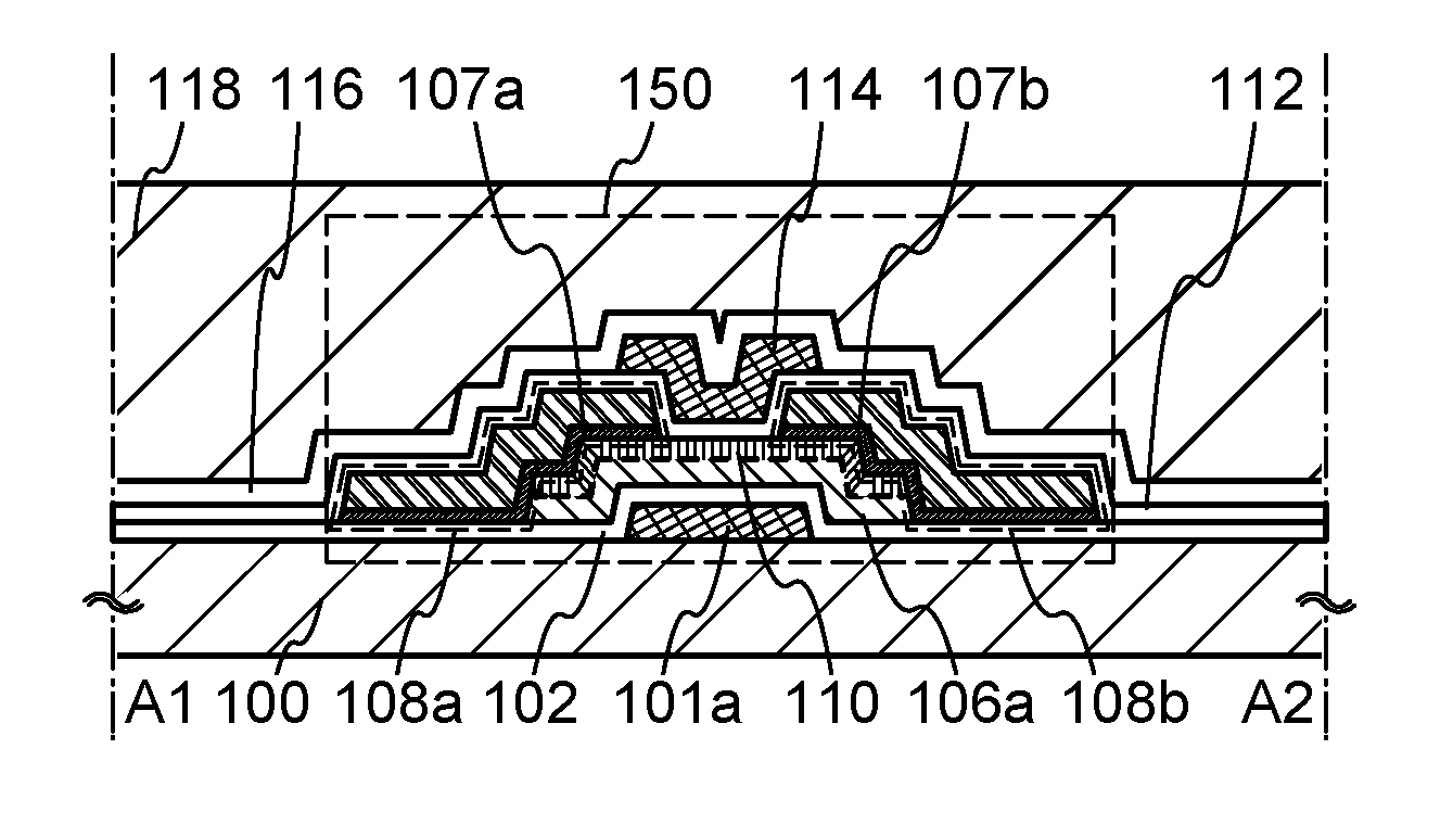
[0063]FIGS. 1A and 1B are cross-sectional views each illustrating a transistor 150 which is an example of a structure of a semiconductor device. Note that the transistor 150 is an n-channel transistor here; alternatively, a p-channel transistor may be used.

[0064]The transistor 150 includes an oxide semiconductor layer 106a provided over a substrate 100 with an insulating layer 102 interposed therebetween, a crystalline region 110 in the oxide semiconductor layer 106a, a source or drain electrode layer 108a and a source or drain electrode layer 108b electrically connected to the oxide semiconductor layer 106a, a gate insulating layer 112 covering the oxide se...

embodiment 2

[0211]In this embodiment, semiconductor devices having structures different from the semiconductor devices of the above embodiment, and a manufacturing method thereof will be described with reference to FIGS. 17A and 17B, FIGS. 18A to 18C, FIGS. 19A to 19C, FIGS. 20A to 20D, FIGS. 21A to 21C, and FIGS. 22A to 22C. Note that the structures described in this embodiment are similar to the structures described in the above embodiment in many points; therefore, only different points will be mainly described below.

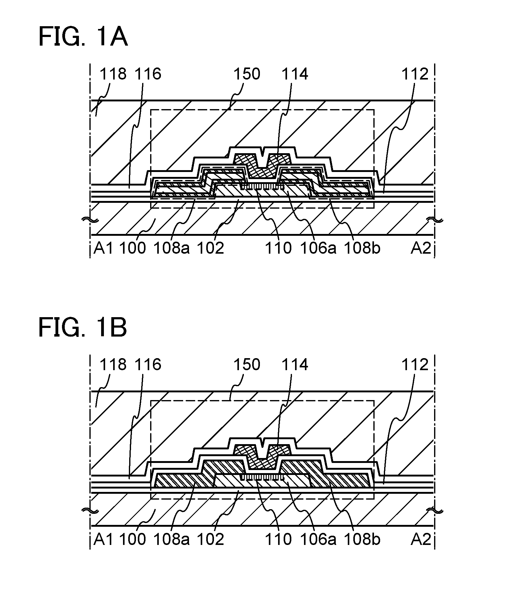
[0212]FIGS. 17A and 17B are cross-sectional views each illustrating a transistor 150 which is an example of a structure of a semiconductor device.

[0213]A point different from the structures of FIGS. 1A and 1B is that a gate electrode layer 101a is provided below the oxide semiconductor layer 106a. In other words, the transistor 150 illustrated in FIG. 17A or 17B includes a gate electrode layer 101a over a substrate 100, an insulating layer 102 covering the gate electrode layer 1...

embodiment 3

[0255]In this embodiment, examples of electronic devices each including the semiconductor device according to any of the above-described embodiments will be described with reference to FIGS. 23A to 23F. The semiconductor device according to any of the above embodiments has unprecedented excellent characteristics. Therefore, an electronic device with a novel structure can be provided by using the semiconductor device.

[0256]FIG. 23A illustrates a notebook personal computer including the semiconductor device according to any of the above embodiments, and includes a main body 301, a housing 302, a display portion 303, a keyboard 304, and the like. The semiconductor device according to the disclosed invention is integrated, mounted on a circuit board or the like, and incorporated in the housing 302. In addition, the semiconductor device according to the disclosed invention can be applied to the display portion 303. By applying the semiconductor device according to the disclosed invention...


PUM


Abstract

A semiconductor device includes an oxide semiconductor layer including a crystalline region over an insulating surface, a source electrode layer and a drain electrode layer in contact with the oxide semiconductor layer, a gate insulating layer covering the oxide semiconductor layer, the source electrode layer, and the drain electrode layer, and a gate electrode layer over the gate insulating layer in a region overlapping with the crystalline region. The crystalline region includes a crystal whose c-axis is aligned in a direction substantially perpendicular to a surface of the oxide semiconductor layer.

Description

TECHNICAL FIELD[0001]A technical field of the disclosed invention relates to a semiconductor device including an oxide semiconductor and a manufacturing method of the semiconductor device. Note that semiconductor devices herein refer to general elements and devices which function by utilizing semiconductor characteristics.BACKGROUND ART[0002]A field-effect transistor is one of the most widely-used semiconductor elements. A variety of materials are used for field-effect transistors according to their uses. In particular, semiconductor materials including silicon are frequently used.[0003]A field-effect transistor including silicon has characteristics satisfying the needs for a variety of uses. For example, single crystal silicon is used for an integrated circuit or the like which needs to be operated at a high speed, whereby the need is satisfied. Further, amorphous silicon is used for an object which needs to have a large area, such as a display device, whereby the need can be satis...

Claims


Application Information

Patent Timeline
Patent Type & Authority Applications(United States)
IPC IPC(8): H01L29/786H01L21/336
CPCH01L27/1225H01L29/045H01L29/66969H01L29/78696H01L29/7869H01L29/04H01L29/78693H01L29/24H01L29/78648
Inventor YAMAZAKI, SHUNPEI
Owner SEMICON ENERGY LAB CO LTD
Why Eureka
Try Eureka