Lead frame, its manufacturing method, and semiconductor light emitting device using the same

a manufacturing method and semiconductor technology, applied in the manufacture of semiconductor devices, cables/conductors, electrical equipment, etc., can solve the problems of poor heat radiating properties, so as to achieve excellent reliability, high heat radiating properties, and the effect of high cos

Inactive Publication Date: 2011-06-09
TOPPAN PRINTING CO LTD
View PDF7 Cites 45 Cited by
  • Summary
  • Abstract
  • Description
  • Claims
  • Application Information

AI Technical Summary

Benefits of technology

[0014]When a ceramic substrate is used as a device carrying substrate having an LED device carried and mounted thereon, for example, its heat radiating property is preferable and its reliability is also excellent but it has a disadvantage that its cost is high. When a printed circuit board is used as the device carrying substrate, it has a disadvantage that an epoxy resin used as a base material of the printed circuit board is not excellent in heat radiating property. A printed circuit board having a metal plate made of Cu (copper) or Al (aluminum) inserted in the inner layer of the board has to be employed to eliminate the disadvantage. Further, in order to reflect a light emitted from the LED device at a high light reflectivity and to secure a high optical gain, there was needed a step of applying an optically-reflective ceramic ink on a light reflecting surface of the substrate having a light emitting diode mounted thereon.

Problems solved by technology

When a ceramic substrate is used as a device carrying substrate having an LED device carried and mounted thereon, for example, its heat radiating property is preferable and its reliability is also excellent but it has a disadvantage that its cost is high.
When a printed circuit board is used as the device carrying substrate, it has a disadvantage that an epoxy resin used as a base material of the printed circuit board is not excellent in heat radiating property.
When a lead frame substrate made of metal thin plate is used as a device carrying substrate having an LED device carried and mounted thereon, it has a disadvantage that a heat radiating property is poor, and there is a need to secure a high optical gain (high light reflectivity in the light irradiating direction) of the LED device.
There has been a disadvantage that although the lead frame substrate system is employed, a satisfactory heat radiation for the mounting substrate surface from the LED device cannot be secured, which leads to an insufficient heat radiating property.
The printed circuit board or the lead frame substrate other than the ceramic substrate is poor in heat radiating property and has a disadvantage that its manufacturing method or steps are more complicated than a method for manufacturing a semiconductor light emitting device using a ceramic substrate.

Method used


Image

  • Lead frame, its manufacturing method, and semiconductor light emitting device using the same
  • Lead frame, its manufacturing method, and semiconductor light emitting device using the same
  • Lead frame, its manufacturing method, and semiconductor light emitting device using the same

Examples


first embodiment

[0070]First, a first embodiment of the present invention will be described below with reference to FIGS. 1, 2, 3, 4 and 5.

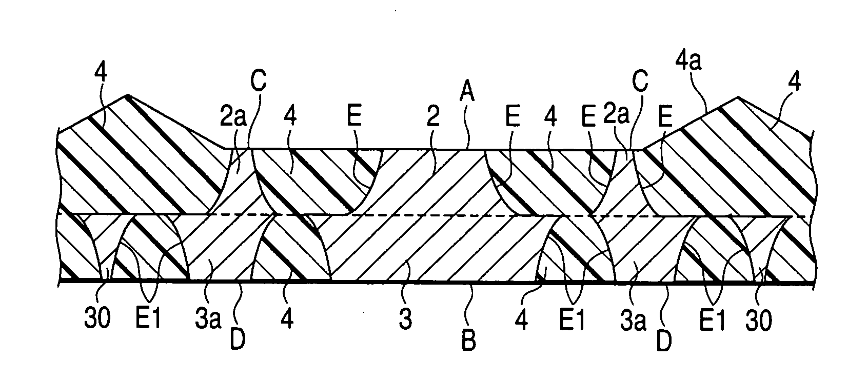
[0071]A lead frame 1 according to the present embodiment is formed by punching a base material having a metallic plate shape through a press mold. In other words, as shown in FIGS. 3 and 5, the lead frame 1 is formed by punching the base material having a metallic plate shape and a thickness t1 through a press mold. The lead frame 1 is formed of an upper structure pattern having a thickness t2 at the surface (a mounting surface of a light emitting diode 10) and a lower structure pattern having a thickness t3 at the lower surface. The upper structure and the lower structure are made of the same metallic thin plate to be integrated with each other. The lead frame 1 is made of a copper thin plate, iron / nickel alloy thin plate or copper / nickel / tin metallic thin plate. However, it is preferable to use copper or copper alloy having high heat conductivity for a metal ma...

second embodiment

[0102]Next, a second embodiment of the present invention will be described below with reference to FIGS. 7, 8 and 9.

[0103]A lead frame 1 according to the present embodiment is formed by photoetching a base material having a metallic thin plate shape. In other words, as shown in FIGS. 7, 8 and 9, the lead frame 1 is formed by photoetching the base material having a thickness t1 and a metallic thin plate shape from both sides. The lead frame 1 is formed of an upper structure pattern having a thickness t2 on the surface (a mounting surface of a light emitting diode 10) and a lower structure pattern having a thickness t3 at the lower surface. Since being made of the same metallic thin plate, the upper structure and the lower structure are integrated. A plate-shaped copper thin plate, an iron / nickel alloy thin plate, or a copper / nickel / tin metallic thin plate is used for the material of the lead frame 1. However, it is more preferable to use copper or copper alloy having high heat conduc...

third embodiment

[0144]Next, a lead frame for a semiconductor light emitting device according to a third embodiment of the present invention will be described below with reference to FIGS. 10, 11A and 11B.

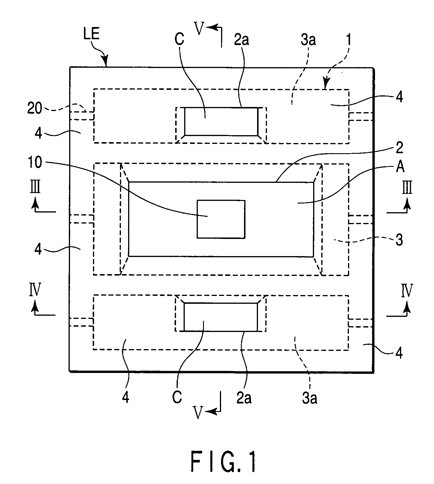
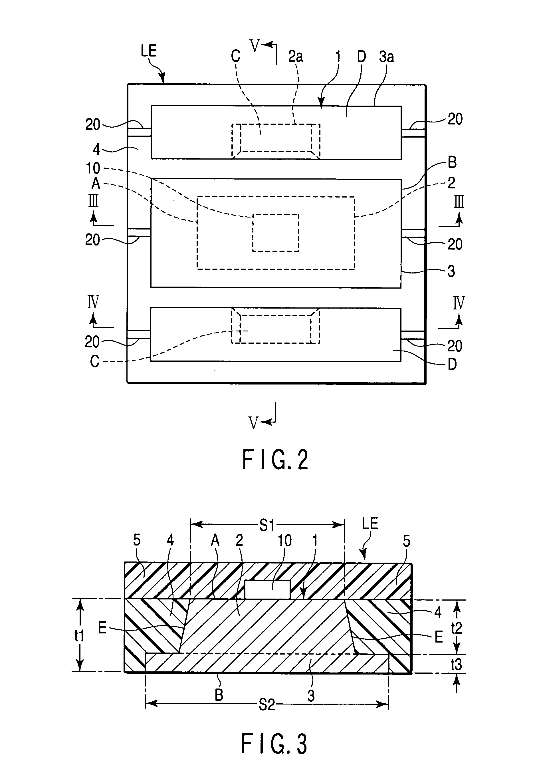
[0145]As shown in FIG. 10, in the lead frame for a semiconductor light emitting device according to the present embodiment, a pad part 2 and a lead part 2a in a lead frame 1 are assumed as a unit frame in which both surfaces are in the same plane (a dotted line Z in FIG. 10 denotes unit frame). The lead frame for a semiconductor light emitting device is manufactured with a branch-shaped or belt-shaped metal material by using a multi-faced lead frame ML in which multiple unit frames are arranged side by side in the longitudinal and lateral directions.

[0146]As shown in FIG. 10, a lattice-shaped frame called tie bar 30 is formed, for example. The tie bar 30 can prevent the lead frame 1 from coming off the metal material after etching or punching using a press mold. The unit frame is formed to be conne...


PUM


Abstract

A lead frame comprises on a same plane, a pad part including an LED chip mounting upper surface A on which at least an LED chip is to be mounted, and a lead part including an electric connection area C in which an electric connection with the LED chip is made. A relationship between an area S1 of the mounting upper surface of the pad part 2 and an area S2 of a radiating lower surface opposite to the mounting upper surface is represented by 0<S1<S2. Side surfaces of the pad part between the mounting upper surface and the radiating lower surface are provided with stepped parts or tapered parts which spread in a direction from the mounting upper surface toward the radiating lower surface and hold a resin-filled during molding.

Description

CROSS REFERENCE TO RELATED APPLICATIONS[0001]This is a Continuation Application of PCT Application No. PCT / JP2009 / 068921, filed Nov. 5, 2009, which was published under PCT Article 21(2) in Japanese.[0002]This application is based upon and claims the benefit of priority from prior Japanese Patent Applications No. 2008-286265, filed Nov. 7, 2008; No. 2009-045460, filed Feb. 27, 2009; and No. 2009-120675, filed May 19, 2009, the entire contents of all of which are incorporated herein by reference.BACKGROUND OF THE INVENTION[0003]1. Field of the Invention[0004]The present invention relates to a lead frame having an LED (Light Emitting Diode) carried and mounted thereon, its manufacturing method, and a semiconductor light emitting device using the same.[0005]2. Description of the Related Art[0006]Generally, a lead frame having an electronic device such as a semiconductor integrated circuit or an LED device carried and mounted thereon is manufactured of a lead frame metal thin plate made ...

Claims


Application Information

Patent Timeline
Patent Type & Authority Applications(United States)
IPC IPC(8): H01L33/62H01L33/60H01L33/48H01L21/48H01L21/027
CPCH01L21/4828H01L33/486H01L33/60H01L33/62H01L33/642H01L24/97H01L2924/01055H01L2224/45144H01L2924/12041H01L2224/48091H01L2224/48247H01L2924/00H01L2924/00014H01L2924/14H01L2924/15787H01L2924/181
Inventor YOSHIOKA, OSAMUMOTOMURA, HITOSHITSUKAMOTO, TAKEHITO
Owner TOPPAN PRINTING CO LTD
Why Eureka
Try Eureka