Multifunctional heater/chiller pedestal for wide range wafer temperature control

Active Publication Date: 2011-06-23
APPLIED MATERIALS INC
View PDF11 Cites 163 Cited by
  • Summary
  • Abstract
  • Description
  • Claims
  • Application Information

AI Technical Summary

Benefits of technology

[0009]Embodiments of the invention generally relate to a semiconductor processing chamber and, more specifically, a heated support pedestal for a semiconductor processing chamber. In one embodiment, a pedestal for a semiconductor processing chamber is provided. The pedestal comprises a substrate support comprising a conductive material and having a support surface for receiving a substrate, a resistive heater encapsulated within the substrate support, a hollow shaft coupled to the substrate support at a first end and to a mating interface at a second end, the hollow shaft comprising a shaft body having a hollow core, and a cooling channel assembly encircling the hollow core and disposed within the shaft body for removing heat from the pedestal via an internal cooling path, wherein the substrate support has a heat control gap positioned between the heating element and the ring-shaped cooling channel.
[0010]In another embodiment, a pedestal for a semiconductor processing chamber is provided. The pedestal comprises a substrate support comprising a conductive material and having a support surface for receiving a substrate, a hollow shaft coupled with the substrate support comprising a shaft body having a hollow core, and an active cooling system providing for active control of the temperature of a substrate positioned on the support surface comprising a heating element encapsulated within the substr

Problems solved by technology

Conventional supports with embedded heaters often have numerous hot and cold spots which affect the quality of films deposited on the substrate.
When heated, conventional substrate support pedestals are very likely to bow up

Method used


Image

  • Multifunctional heater/chiller pedestal for wide range wafer temperature control
  • Multifunctional heater/chiller pedestal for wide range wafer temperature control
  • Multifunctional heater/chiller pedestal for wide range wafer temperature control

Examples


Example

[0023]To facilitate understanding, identical reference numerals have been used, where possible, to designate identical elements that are common to the figures. It is contemplated that elements and features of one embodiment may be beneficially incorporated in other embodiments without further recitation.

DETAILED DESCRIPTION

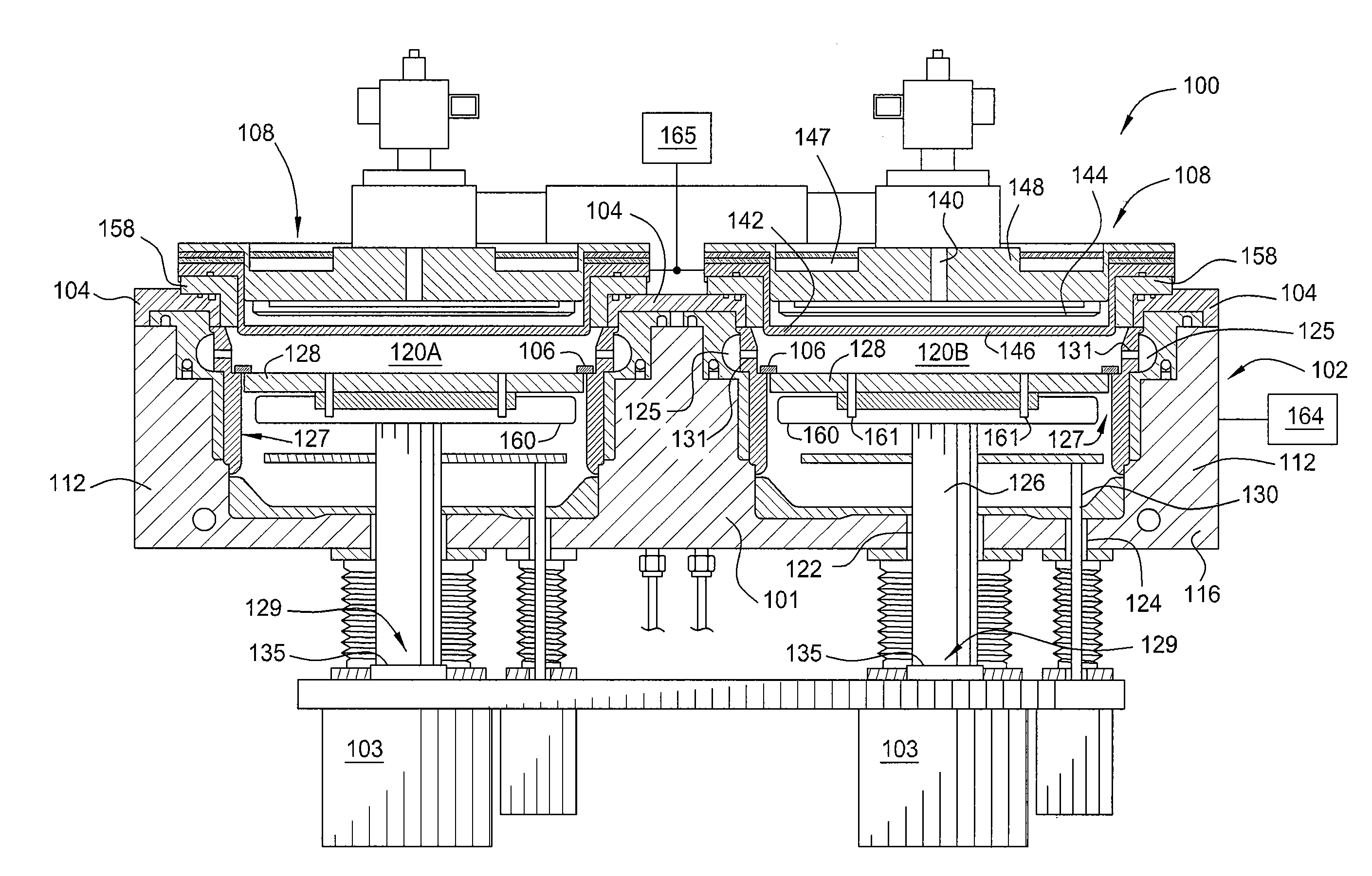
[0024]Embodiments of the invention generally relate to a semiconductor processing chamber and, more specifically, a heated support pedestal for a semiconductor processing chamber. Embodiments of the present invention are illustratively described below in reference to plasma chambers. In one embodiment, the plasma chamber is utilized in a plasma enhanced chemical vapor deposition (PECVD) system. Examples of PECVD systems that may be adapted to benefit from the embodiments described herein include a PRODUCER® SE CVD system, a PRODUCER® GT™ CVD system or a DXZ® CVD system, all of which are commercially available from Applied Materials, Inc., Santa Clara, Calif. The P...


PUM

PropertyMeasurementUnit
Lengthaaaaaaaaaa
Lengthaaaaaaaaaa
Lengthaaaaaaaaaa

Abstract

Embodiments of the invention generally relate to a semiconductor processing chamber and, more specifically, a heated support pedestal for a semiconductor processing chamber. In one embodiment, a pedestal for a semiconductor processing chamber is provided. The pedestal comprises a substrate support comprising a conductive material and having a support surface for receiving a substrate, a resistive heater encapsulated within the substrate support, a hollow shaft coupled to the substrate support at a first end and a mating interface at an opposing end, the hollow shaft comprising a shaft body having a hollow core, and a cooling channel assembly encircling the hollow core and disposed within the shaft body for removing heat from the pedestal via an internal cooling path, wherein the substrate support has a heat control gap positioned between the heating element and the ring-shaped cooling channel.

Description

BACKGROUND OF THE INVENTION[0001]1. Field of the Invention[0002]Embodiments of the invention generally relate to a semiconductor processing chamber and, more specifically, a heated support pedestal for a semiconductor processing chamber.[0003]2. Description of the Related Art[0004]Semiconductor processing involves a number of different chemical and physical processes whereby minute integrated circuits are created on a substrate. Layers of materials which make up the integrated circuit are created by processes including chemical vapor deposition, physical vapor deposition, epitaxial growth, and the like. Some of the layers of material are patterned using photoresist masks and wet or dry etching techniques. The substrates utilized to form integrated circuits may be silicon, gallium arsenide, indium phosphide, glass, or other appropriate materials.[0005]In the manufacture of integrated circuits, plasma processes are often used for deposition or etching of various material layers. Plasm...

Claims


Application Information

Patent Timeline
IPC IPC(8): H05B3/68
CPCH01L21/68792H01L21/67109C23C16/458H01L21/205H01L21/67248H01L21/68
Inventor YAP, LIPYEOWNGUYEN, TUAN ANHDU BOIS, DALE R.BALUJA, SANJEEVNOWAK, THOMASROCHA-ALVAREZ, JUAN CARLOSZHOU, JIANHUA
Owner APPLIED MATERIALS INC
Why Eureka
Try Eureka