Light emitting diode package and method of fabricating the same

a technology of led packages and led components, which is applied in the direction of semiconductor/solid-state device manufacturing, electrical equipment, semiconductor devices, etc., can solve the problems of reduced processing yield, complex bonding process, and open defects in the wires, so as to improve the lamination efficiency of led packages and prevent problems

Active Publication Date: 2011-06-23
LG DISPLAY CO LTD
View PDF9 Cites 26 Cited by
  • Summary
  • Abstract
  • Description
  • Claims
  • Application Information

AI Technical Summary

Benefits of technology

An object of the present invention is to improve lamination efficiency of an LED package.
Another object of the present invention is to prevent problems during a bonding process for an LED package.

Problems solved by technology

Unfortunately, there can be an open defect on the wires 70.
The bonding process is very complicated such that processing yield is also decreased.

Method used


Image

  • Light emitting diode package and method of fabricating the same
  • Light emitting diode package and method of fabricating the same
  • Light emitting diode package and method of fabricating the same

Examples


Embodiment Construction

Reference will now be made in detail to the preferred embodiments, examples of which are illustrated in the accompanying drawings.

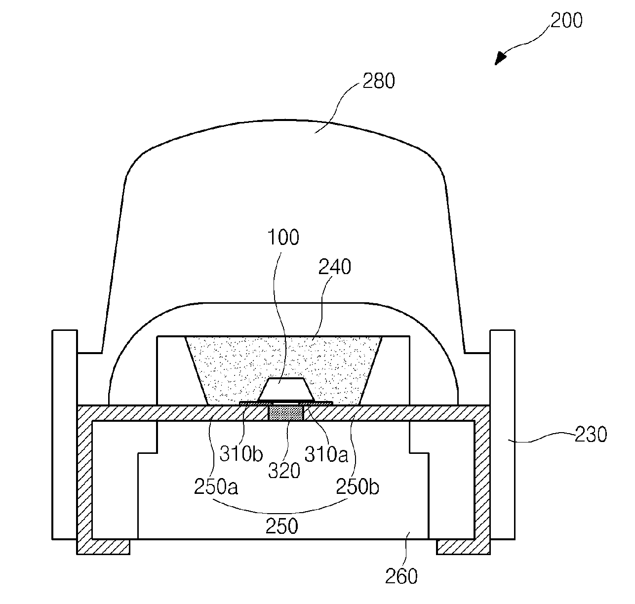
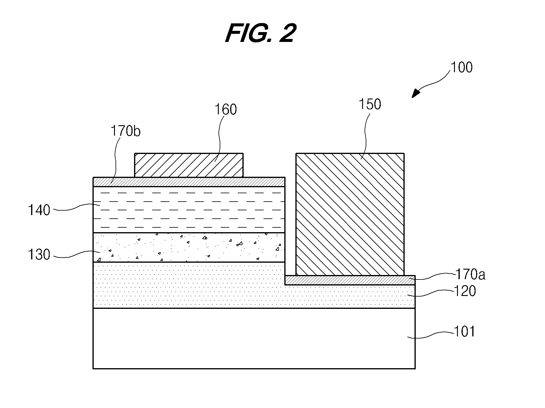
FIG. 2 is a schematic cross-sectional view of an LED chip according to an exemplary embodiment of the present invention. As shown in FIG. 2, an LED chip 100 includes a substrate 101, an n-type semiconductor layer 120, an active layer 130, a p-type semiconductor layer 140, first and second reflection plates 170a and 170b, a first electrode 150 and a second electrode 160. The p-type semiconductor layer 140 and the n-type semiconductor layer 120 form a forward-biased junction. The substrate 101 may be formed of a transparent material, such as sapphire. Alternatively, zinc oxide (ZnO), gallium nitride (GaN), silicon carbide (SiC) or aluminum nitride (AlN) may be used for the substrate 101.

The n-type semiconductor layer 120 is formed on the substrate 101. To improve a lattice junction property, a buffer layer (not shown) may be formed between the substrate 101...


PUM


Abstract

A light emitting diode (LED) package and a method of manufacturing a LED package is provided. The LED package includes a case having first and second lead frames disposed through the case; an LED chip disposed on the case, the LED chip having first and second electrodes directly connected to the first and second lead frames through a eutectic bond, respectively; and a lens disposed over the case covering the LED chip.

Description

The present application claims the benefit of Korean Patent Application No. 10-2009-0127788, filed in Korea on Dec. 21, 2009, which is hereby incorporated by reference.BACKGROUND OF THE INVENTION1. Field of the InventionThe present invention relates to a light emitting diode (LED) package, and more particularly, to an LED package being capable of preventing problems during a bonding process and a method of fabricating the LED package.2. Discussion of the Related ArtRecently, LEDs are widely used because their characteristic of small size, low power consumption and high reliability. For example, LEDs are used for electric illumination and light sources in display devices. Particularly, to replace fluorescent lamps, LEDs that emits white light can be used. LEDs that emit white light are also being introduced for backlight units in liquid crystal display (LCD) devices.FIG. 1 is a cross-sectional view of a related art LED package. As shown in FIG. 1, the LED package 10 includes an LED c...

Claims


Application Information

Patent Timeline
Patent Type & Authority Applications(United States)
IPC IPC(8): H01L33/10H01L21/52
CPCH01L33/486H01L33/504H01L33/58H01L33/62H01L2933/0066H01L2224/48091H01L2924/01322H01L2924/00014H01L2924/00
Inventor KANG, SIN-HOKIM, TAE-HUNJANG, SEUNG-HOHAN, KYOUNG-BOCHOI, JAE-YONG
Owner LG DISPLAY CO LTD
Why Eureka
Try Eureka