Electric double layer capacitor and method for manufacturing the same
- Summary
- Abstract
- Description
- Claims
- Application Information
AI Technical Summary
Benefits of technology
Problems solved by technology
Method used
Image
Examples
example 1
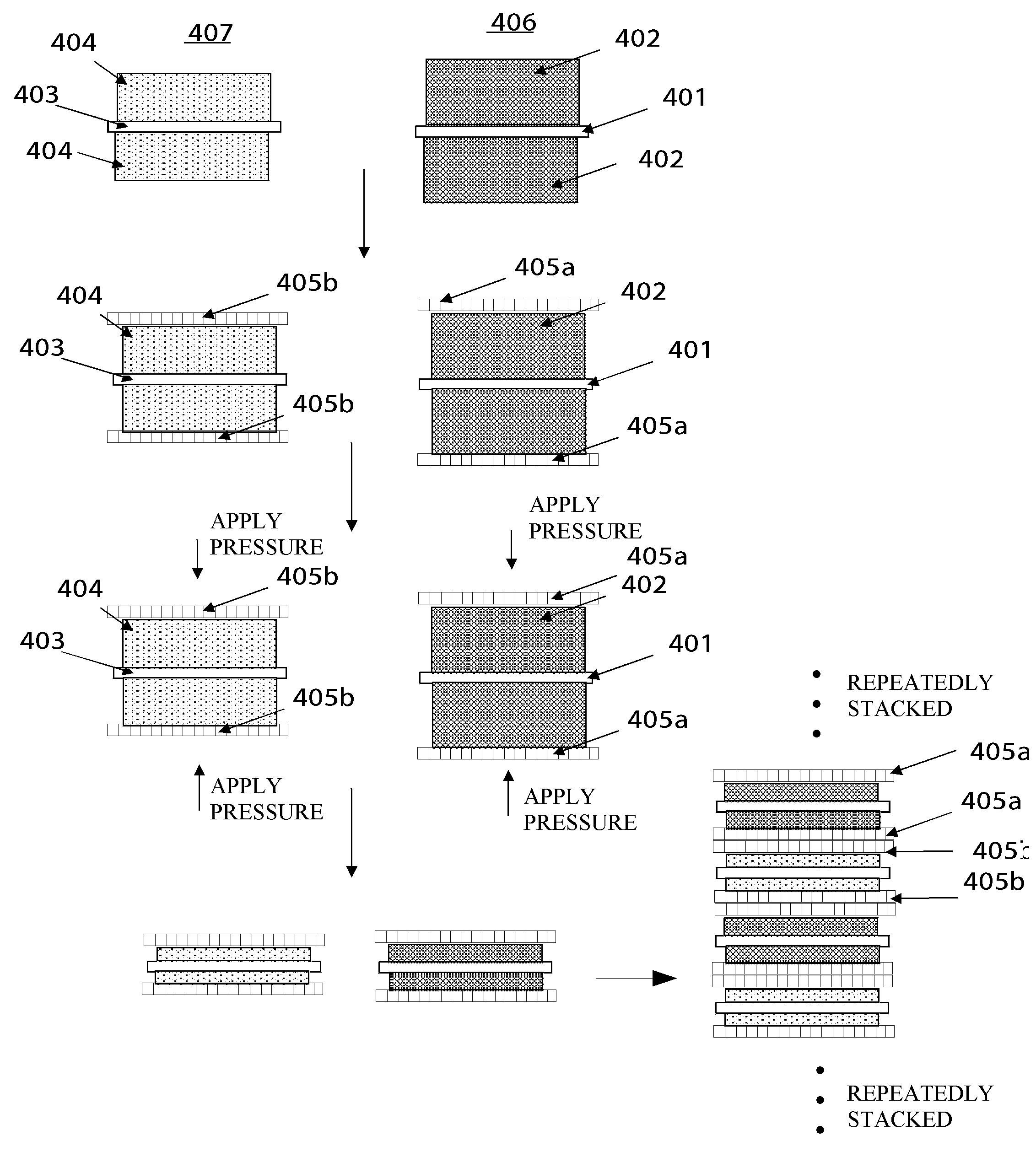
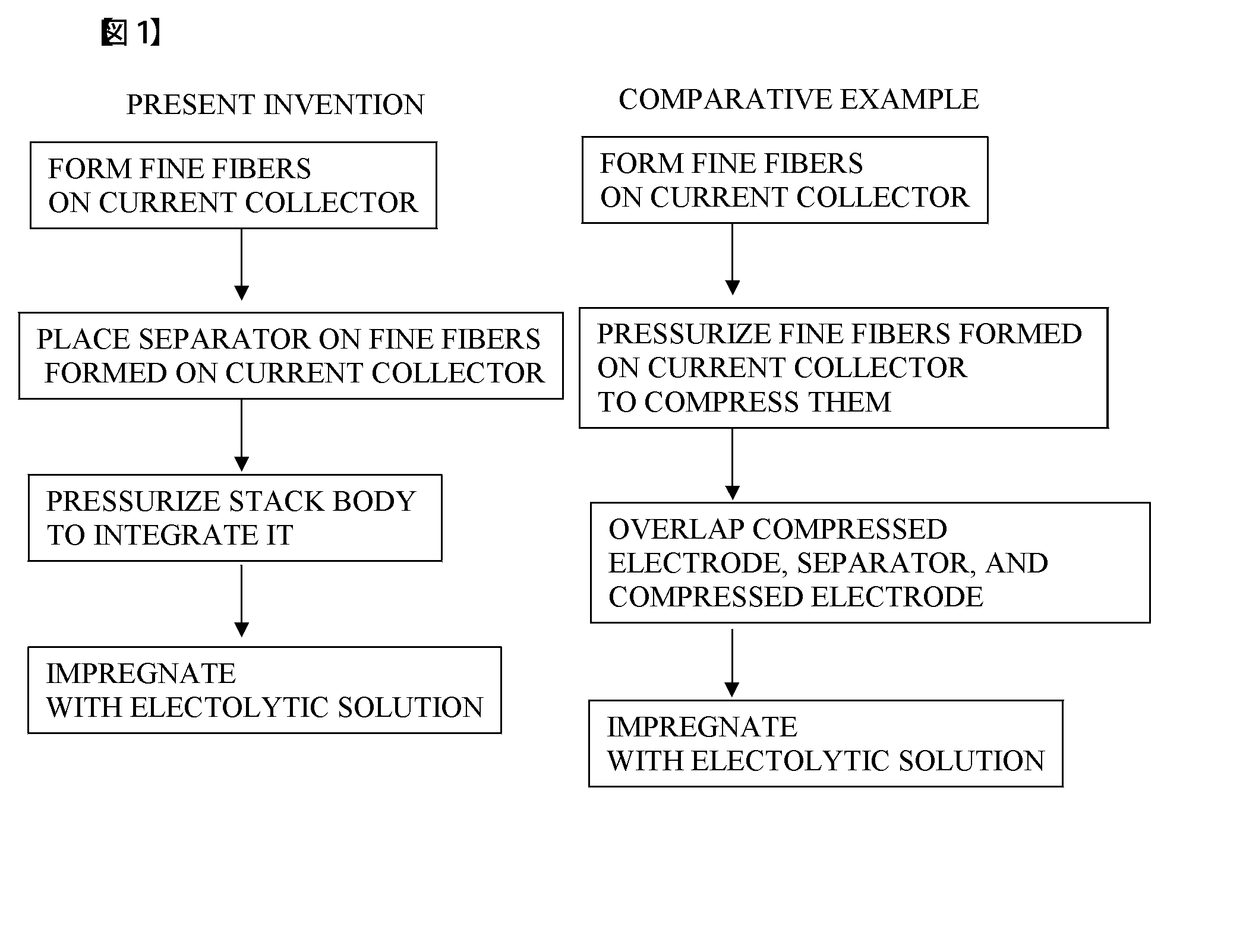
[0079]In Example 1, the separator was placed on the fine fibers standing on the surface of the current collector, and pressure is applied to the stack body including the polar plate and the separator. Thus, the electrode for the electric double layer capacitor was manufactured. The carbon nanotubes were used as the fine fibers.
[0080]The method for forming the carbon nanotubes on the current collector is the same as the method of Comparative Example 1, so that an explanation thereof is omitted.
[0081]The Si wafer was placed on the carbon nanotubes, and the carbon nanotubes were compressed by pressure (4 MPa) by which the carbon nanotubes were not transferred to the Si wafer.
[0082]Two current collectors were placed so as to sandwich a polypropylene separator having a thickness of 25 μm such that the carbon nanotubes formed on these two current collectors were opposed to each other. Then, these were pressurized by pressure of 50 MPa using the press device. In order to equally distribute...
example 2
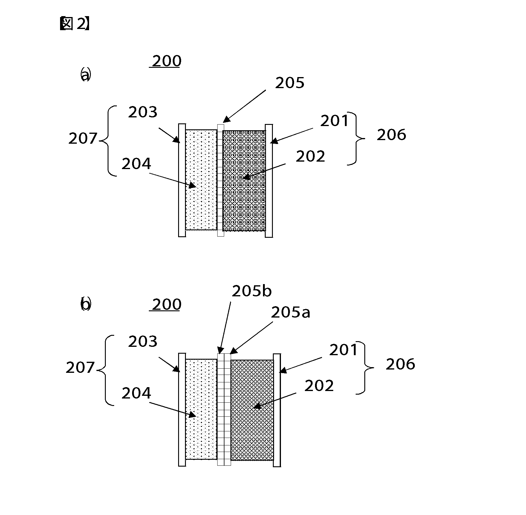
[0086]In Example 2, the electric double layer capacitor was manufactured by using the electric double layer capacitor electrode which was manufactured in Example 1 such that the positive electrode, the separator, and the negative electrode were pressure bonded to be integrated with one another.
[0087]The electric double layer capacitor electrode was immersed in the electrolytic solution. The electrolytic solution was prepared by dissolving tetrafluoroboric acid tetraethylammonium in propylene carbonate. The concentration of tetrafluoroboric acid tetraethylammonium was 0.7 mol / l. Next, the pressure was reduced to a level that the electrolytic solution did not boil, and the electrolytic solution permeated the active material.
[0088]A cyclic voltammogram measurement was carried out at a voltage sweep rate of 40 mV / sec in a voltage range from 0V to 3.5V with respect to the electrode impregnated with the electrolytic solution as above. A graph obtained by the measurement is shown in FIG. 1...
example 3
[0091]Example 3 will explain an example in which: the positive electrode manufactured in Example 1 and the positive electrode separator were pressure bonded to be integrated with each other; the negative electrode manufactured in Example 1 and the negative electrode separator were pressure bonded to be integrated with each other; and the electric double layer capacitor was manufactured by overlapping these separators each other.
[0092]The compressed stack body manufactured as in Example 1 and including the positive electrode and the positive electrode separator and the compressed stack body manufactured as in Example 1 and including the negative electrode and the negative electrode separator overlapped each other such that the separators thereof were opposed to each other. This was fixed by a Teflon plate and immersed in the electrolytic solution. The method for immersing was the same as the method described in Example 2, so that an explanation thereof is omitted.
[0093]The capacitor ...
PUM
| Property | Measurement | Unit |
|---|---|---|
| Pressure | aaaaa | aaaaa |
| Pressure | aaaaa | aaaaa |
| Diameter | aaaaa | aaaaa |
Abstract
Description
Claims
Application Information


