Heat-resistant adhesive sheet for substrateless semiconductor package fabrication and method for fabricating substrateless semiconductor package using the adhesive sheet

Inactive Publication Date: 2011-06-23
NITTO DENKO CORP
View PDF19 Cites 23 Cited by
  • Summary
  • Abstract
  • Description
  • Claims
  • Application Information

AI Technical Summary

Benefits of technology

[0028]The present invention provides a heat-resistant adhesive sheet 2 for semiconductor device fabrication that is used in a substrateless semiconductor package fabrication method (such as WLP fabrication method) that does not use a metal lead frame, and a semiconductor device fabrication method that uses the sheet. According to the present invention, when substrateless semiconductor chips that do not use a metal lead frame are encapsulated with resin, the chips are held so that the chip

Problems solved by technology

Furthermore, since the chips need to be unfixed after the chips have been encapsulated with resin and formed into individual packages, the supporter need to be removable, instead of permanent bonding fixation.
Obviously, the method is not intended for substrateless semiconductor devices and the adhesive layer is chosen by taking into consideration the adhesiveness to a substrate.
The following problems can arise with the following method for fabricating a substrateless semiconductor package using an adhesive sheet as a temporary supporter, which do not arise with fabrication of semiconductor packages using a lead frame.
Consequently, the positions of chips encapsulated in the packages resulting from dicing would vary from one package to another and a subsequent ele

Method used


Image

  • Heat-resistant adhesive sheet for substrateless semiconductor package fabrication and method for fabricating substrateless semiconductor package using the adhesive sheet
  • Heat-resistant adhesive sheet for substrateless semiconductor package fabrication and method for fabricating substrateless semiconductor package using the adhesive sheet
  • Heat-resistant adhesive sheet for substrateless semiconductor package fabrication and method for fabricating substrateless semiconductor package using the adhesive sheet

Examples


working examples

[Measuring Method]

[0116]Measurements and evaluations in working examples and comparative examples were made as follows.

[0117]Initial adhesion strength to SUS: Peel adhesion strength to a SUS304BA plate at an angle of 180° at room temperature

[0118]Adhesion strength to SUS304 after heating: Peel adhesion strength at an angle of 180° after attached to a SUS304BA plate and heated at 150° C. for 60 minutes

[0119]Adhesion strength to SUS304 at 175° C.: Peel adhesion strength to a SUS304BA plate at 175° C.

[0120]Peel strength from package: Peel adhesion strength at an angle of 180° when the adhesive sheet is peeled from the package

[0121]Chip displacement: Displacement from the initial position of a chip measured with a digital microscope after package fabrication

[0122]Adhesive deposit: The surface of the package was visually checked for adhesive deposits after the adhesive sheet was peeled off.

[0123]The term “part” in the following description means “part by weight”.

working example 1

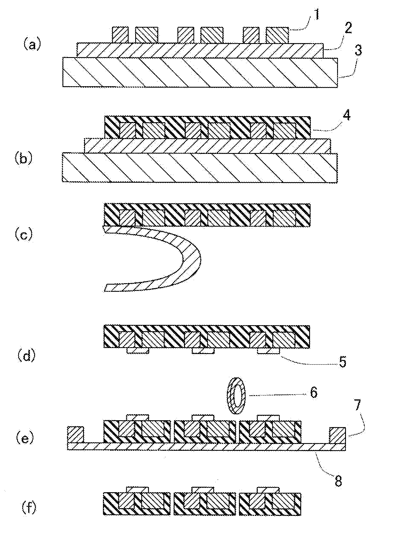
[0124]3 pts.wt. of acrylic acid monomer as a component monomer was blended with 100 pts.wt. of butyl acrylate monomer to derive an acrylic-based copolymer. 3 pts.wt. of an epoxy-based cross-linking agent (Tetrad-C from Mitsubishi Gas Chemical Company, Inc.) and 5 pts.wt. of an isocyanate-based cross-linking agent (Coronate L from Nippon Polyurethane Industry Co., Ltd.) were blended with 100 pts.wt. of the acrylic-based copolymer to prepare an acrylic-based adhesive. 50 pts.wt. of a UV curable compound (UV-1700B from Nippon Synthetic Chemical Industry Co., Ltd.) and 3 pts.wt. of UV curing initiator (Irgacure 651 from NAGASE & CO., LTD.) were added to the acrylic-based adhesive to prepare an adhesive composition.

[0125]Then, the adhesive composition was applied to a 25-μm-thick polyimide film (Kapton 100H from Du Pont-Toray Co., Ltd.) serving as the base material layer, and then dried to prepare a heat-resistant adhesive sheet for semiconductor device fabrication with an adhesive layer...

working example 2

[0136]42 parts of acrylonitrile-butadiene rubber (Nipol 1072) from Zeon Corporation), 53 parts of bisphenol A-type epoxy resin (Epikote 828 from Japan Epoxy Resin Co., Ltd., with a weight per epoxy equivalent of 190 g / eq), and 5 parts of imidazole (C1 1Z from Shikoku Chemicals Corporation) were blended and dissolved in an MEK solvent to a concentration of 35 wt % to prepare a bond solution. The bond solution was applied to a 35-μm-thick copper foil serving as a base material film, and was then dried at 150° C. for 3 minutes to form a bond layer having a bond thickness of 10 μm, thus forming a heat-resistant adhesive sheet for semiconductor device fabrication.

[0137]A 3 mm×3 mm Si wafer chip was placed on the heat-resistant adhesive sheet for semiconductor device fabrication, epoxy-based encapsulation resin powder (GE-740LA from Nitto Denko Corporation) was sprinkled over the sheet and the wafer chip, and then molded by heating at a temperature of 175° C. under a pressure of 3.0 kg / cm...


PUM

PropertyMeasurementUnit
Energyaaaaaaaaaa
Pressureaaaaaaaaaa
Electrical resistanceaaaaaaaaaa

Abstract

The present invention is intended to solve the following problems with a method for fabricating a substrateless semiconductor package using an adhesive sheet as a temporary fixing supporter. A chip can be displaced from a specified position by pressure during resin encapsulation because the chip is not properly held by the adhesive sheet. If such displacement occurs, the relative positional relationship between the chip and an interconnect to be connected to a specified position in a subsequent wiring step also changes by the displacement of the chip from the specified position. Another problem is that if adhesive deposits occur during peeling of the adhesive sheet and the surface of a package is contaminated with the adhesive deposits, adhesive components left on the surface of the chip can inhibit connection between the interconnect and the chip in a subsequent wiring step. To solve these problems, the present invention provides an adhesive sheet for semiconductor device fabrication that is attached to a substrateless semiconductor chip when the chip is encapsulated with resin. The adhesive sheet includes a base material layer and an adhesive layer. The adhesive layer has a specific adhesion strength and peel strength.

Description

BACKGROUND OF THE INVENTION[0001]1. Field of the Invention[0002]The present invention relates to a heat-resistant adhesive sheet for temporarily fixing chips used in a method for fabricating substrateless semiconductor packages that do not use a metal lead frame.[0003]2. Description of the Related Art[0004]Among LSI packaging technologies, Chip Size / Scale Package (CSP) technologies have recently come into attention. Among those technologies, substrateless semiconductor package technology such as Wafer Level Package (WLP) is attractive in terms of packaging density and size reduction. In a WLP fabrication method, multiple semiconductor Si wafer chips orderly arranged without the use of a substrate are encapsulated with an encapsulation resin at a time and then the wafer is diced into individual structures. Thus the method enables packages smaller than conventional ones that use a substrate to be fabricated efficiently.[0005]In such a WLP fabrication method, chips, which are conventio...

Claims


Application Information

Patent Timeline
IPC IPC(8): H01L21/50B32B7/12
CPCH01L21/568Y10T428/287H01L23/3114H01L23/5389H01L24/24H01L24/96H01L2224/24137H01L2924/01013H01L2924/01029H01L2924/01032H01L2924/01033H01L2924/01047H01L2924/01051H01L2924/01079H01L2924/01082H01L2924/01005H01L2924/01006H01L2924/01019H01L2924/01024H01L2924/01042H01L2924/01075H01L2924/01078Y10T428/28H01L23/3107H01L2924/181H01L2924/00
Inventor HOSHINO, SHINJIARIMITSU, YUKIOKIUCHI, KAZUYUKIMURATA, AKIHISA
Owner NITTO DENKO CORP
Why Eureka
Try Eureka