Adjustable CMOS sensor array

a sensor array and cmos technology, applied in the field of semiconductor devices, can solve the problems of large dynamic range and low noise cmos sensors that have not been used, image intensifier devices suffering from increasing fixed pattern noise (fpn), signal to noise ratio (snr) and dynamic range, etc., and achieves the effect of faster ra

Inactive Publication Date: 2011-06-30
IMAGERLABS
View PDF11 Cites 15 Cited by
  • Summary
  • Abstract
  • Description
  • Claims
  • Application Information

AI Technical Summary

Benefits of technology

[0027]If no reset is performed in between consecutive fast sampling operations, an even faster rate can be achieved allowing detecting minute changes in the waveform of the input signal.

Problems solved by technology

However in some extreme applications such as Laser Induced Breakdown Spectroscopy (LIBS) that require ultrafast electronic shutter speeds (referred to as gating), large dynamic range and low noise CMOS sensors have not been used.
For example, Image Intensifier devices suffer from increase in Fixed Pattern Noise (FPN) due to the non-uniformity of the photoelectron gain of the device across the entire imaging area.
That causes reduction in Signal to Noise Ratio (SNR) and Dynamic Range and increases device complexity for FPN correction functionality.
An additional problem is the limited spectral response of the Image Intensifier device, which has poor sensitivity at the longer red wavelengths, UV, and deep blue, a characteristic that is often harmful to the performance of a wide spectra range imaging systems such as Laser Induce Breakdown Spectroscopy (LIBS) or other spectroscopic systems and thus not desired.
Furthermore, an Image Intensifier device suffers from relatively low intra-frame dynamic range due to the high intensifier gain which will cause the CCD to saturate earlier.
This problem is particularly damaging to the Echelle spectrograph that simultaneously provides the strongest lines of the major elements and the weak lines of the trace elements.
The intra-frame dynamic range problem is further convolved by localized dynamic range problems.
The halo unfortunately masks any neighboring lower signals thus reducing the local dynamic range.
As mentioned above, this becomes a severe issue for the Echelle spectrograph that simultaneously provides the strongest lines of the major elements and the weak lines of the trace elements.

Method used


Image

  • Adjustable CMOS sensor array
  • Adjustable CMOS sensor array
  • Adjustable CMOS sensor array

Examples


Embodiment Construction

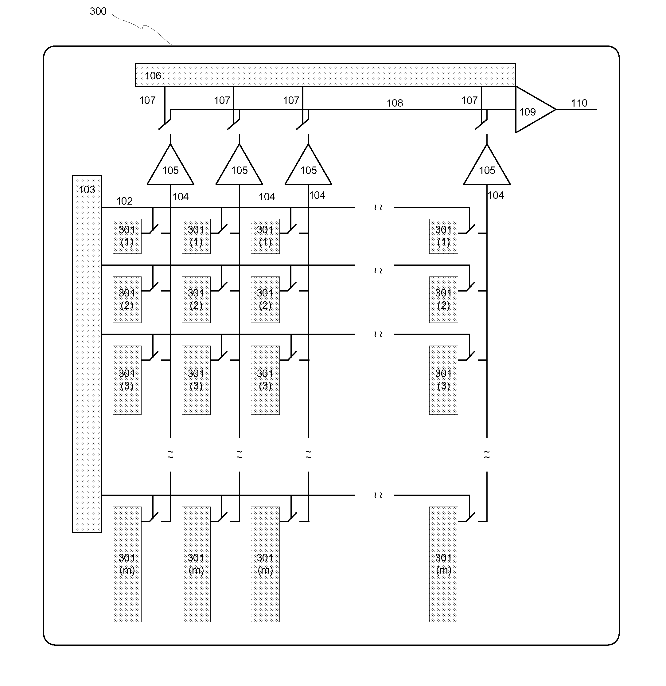
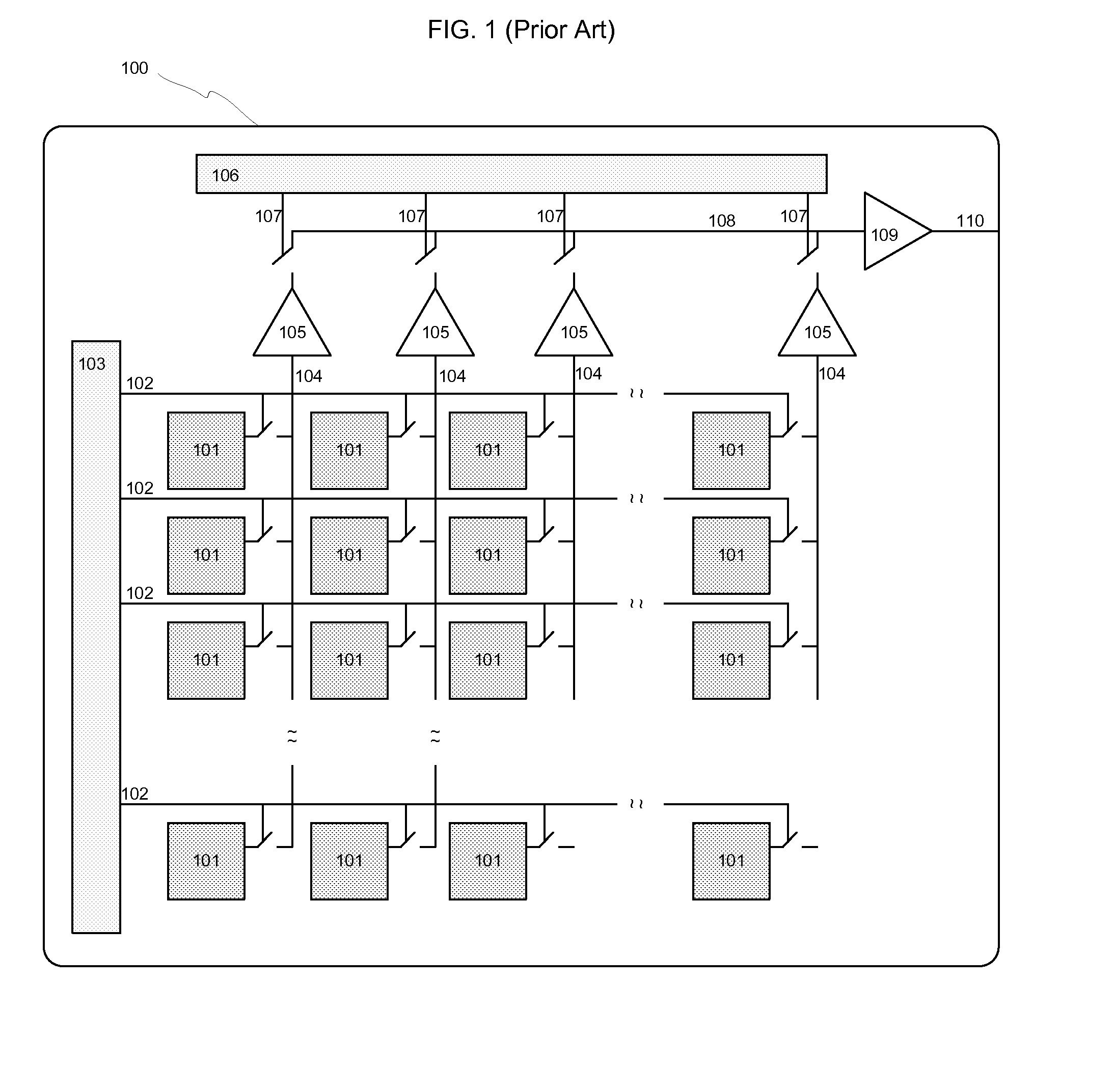
[0042]FIG. 1 is a diagram of a conventional CMOS Pixel sensor 100, which comprises a plurality of square pixels 101 of identical dimensions arranged in a focal plane array. The incoming photons are detected via a photo sensing element in each pixel 101 such as a photodiode or a photogate. The diagram is applicable to both Active Pixel Sensor (APS) and a Passive Pixel Sensor. For an APS, there is at least one additional reset control line going to all pixels (not shown here). The charge is either converted to voltage inside pixels 101 for an APS design or in column bus amplifiers 105. A vertical shift register 103 controls the raw selection via buses (switches) 102, and the voltage (for APS) or charge (for passive pixel) is transferred to the column buffers 105 via a signal line 104. Horizontal shift register 106 controls selection of the output of the column buffers 105 via buses (and switches) 107 and 108. The outputs of the column buffers 105 are then individually selected by the ...


PUM


Abstract

In one aspect, the present invention provides an active pixel sensor array with optimized matching between pixels and strength and frequency of incoming signals such as photons absorbed. The array comprises multiple pixels of individual geometry corresponds to spatial location. Each pixel full-well is adjustable via modifiable pixel conversion gain while maintaining pixel linearity. Furthermore each pixel internally stores multiple of extremely high frequency samples. Variable pixel geometry per row is very advantageous for Echelle spectrograph, where pixel heights are aligned with the spectrograph “order separator” where the resolution changes. In combination with variable geometry, externally adjustable full-well provides for superior spectral line separation in spectroscopy applications. In one embodiment multiple time windows with intermittent resets are stored within each pixel. This feature allows for the detection of extreme high frequency consecutive events without saturation such as may be the case with LIBS (Laser Induced Breakdown Spectroscopy).

Description

CROSS REFERENCE TO RELATED APPLICATION[0001]This application relates to and claims priority to U.S. Provisional Patent Application Ser. No. 61 / 290,118, filed Dec. 24, 2009, which is incorporated by reference in its entirety.BACKGROUND[0002]1. Field of the Invention[0003]The present invention relates to semiconductor devices and, in particular, to complementary metal oxide semiconductor (CMOS) image and mass spectroscopy sensors.[0004]2. Related Art[0005]In the past decade, CMOS sensor arrays and in particular Active Pixel Sensor (APS) arrays for imaging including visible and non-visible applications have been consistently enhanced. Their significantly improved quality with respect to Charge Coupled Devices (CCDs) allows the sensors to be used in varied and challenging applications. A typical CMOS Active Pixel sensor array comprises a focal plane array of evenly spaced and equally sized pixel cells (pixels), where each pixel comprises a light (visible or non visible) detection compon...

Claims


Application Information

Patent Timeline
Patent Type & Authority Applications(United States)
IPC IPC(8): H01L27/146
CPCH04N5/3559H04N5/37452H04N5/3696H04N25/59H04N25/702H04N25/771
Inventor NETER, SARITATLAS, EUGENE
Owner IMAGERLABS
Why Eureka
Try Eureka