

Pixel and organic light emitting display device using the same
- Summary
- Abstract
- Description
- Claims
- Application Information
AI Technical Summary
Benefits of technology
Problems solved by technology
Method used
Image

Examples
first embodiment
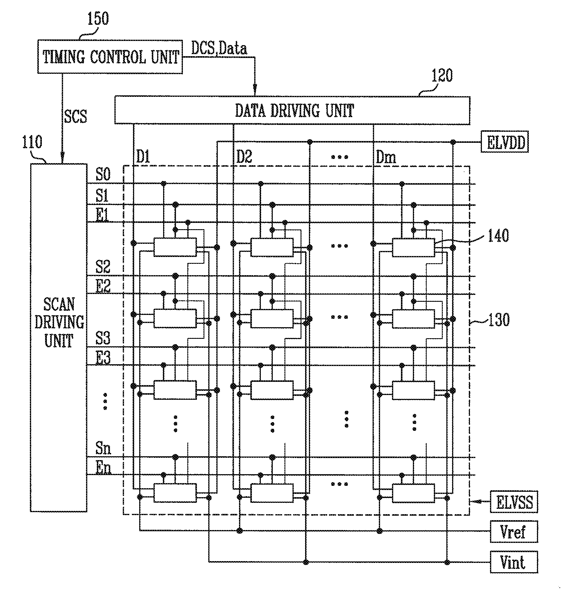
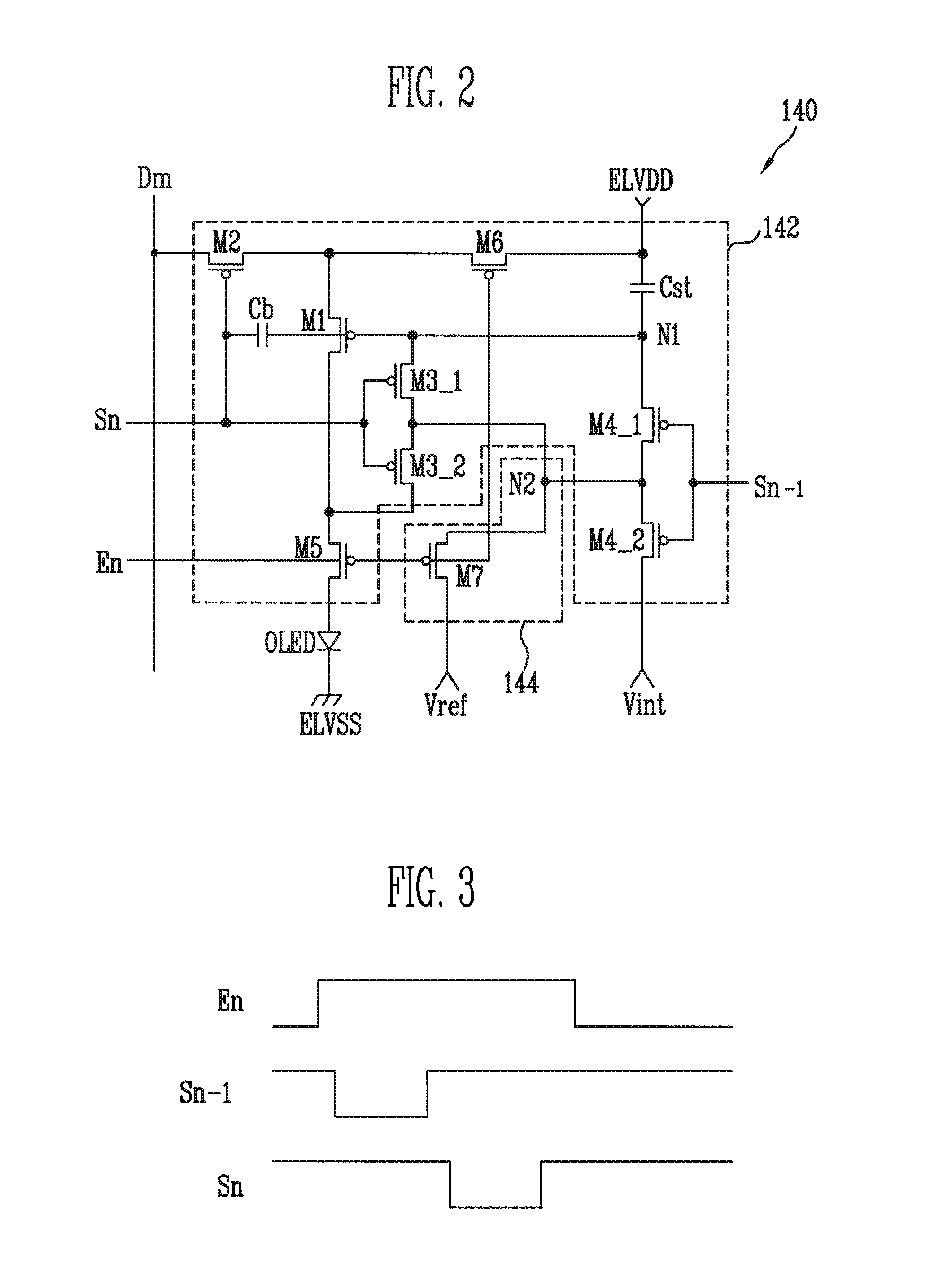
[0038]FIG. 2 is a circuit diagram illustrating the pixel 140 as shown in FIG. 1. For convenience of description, FIG. 2 shows a pixel connected to an (n-1)th scan line Sn-1, an n-th scan line Sn, and an m-th data line Dm.
[0039]Referring to FIG. 2, the pixel 140 according to an embodiment of the present invention includes a pixel circuit 142, which is connected to an organic light emitting diode (OLED), the data line Dm, the scan lines Sn-1 and Sn, and the light emitting control line En, for controlling an amount of current supplied to the OLED, and a leakage current prevention unit 144 electrically connected to a transistor formed on a current leakage path of the pixel circuit 142.
[0040]An anode electrode of the OLED is connected to the pixel circuit 142, and a cathode electrode of the OLED is connected to the second power source ELVSS. As such, the OLED generates light with a corresponding brightness in response to a current supplied from the pixel circuit 142.
[0041]The pixel circu...
second embodiment
[0063]FIG. 4 is a circuit diagram illustrating the pixel of FIG. 1. In the description of FIG. 4, like elements as shown in FIG. 2 will be assigned with like reference numerals and their description will be omitted.
[0064]Referring to FIG. 4, a pixel 140 according to a second embodiment of the present invention includes an OLED, a pixel circuit 142 for controlling the amount of current to be supplied to the OLED, and a leakage current prevention unit 144′ electrically connected to transistors formed on a path of the leakage current in order to minimize or reduce the leakage current.
[0065]The leakage current prevention unit 144′ includes a seventh transistor M7′ connected between the common node of the third transistors M3_1 and M3_2 and the reference power source Vref and an eighth transistor M8 connected between the common node of the fourth transistors M4_1 and M4_2 and the reference power source Vref.
[0066]The seventh transistor M7′ is turned on when the light emitting control sig...
third embodiment
[0067]FIG. 5 is a circuit diagram illustrating the pixel of FIG. 1. In the description of FIG. 5, like elements as shown in FIG. 2 will be assigned with like reference numerals and their description will be omitted.
[0068]Referring to FIG. 5, a pixel 140 according to a third embodiment of the present invention includes an OLED, a pixel circuit 142′ for controlling the amount of current supplied to the OLED, and a leakage current prevention unit 144 electrically connected to transistors formed on a path of the leakage current in order to minimize or reduce the leakage current of the pixel circuit 142′.
[0069]According to the third embodiment of the present invention, in the pixel circuit 142′, a driving transistor includes a plurality of first transistors M1_1, M1_2, and M1_3. That is, the first transistors M1_1, M1_2, and M1_3 are connected in series between the second electrode of the second transistor M2 and the first electrode of the fifth transistor M5, and gate electrodes of the ...
PUM
 Abstract
Description
Claims
Application Information