Fan-out wafer level package with polymeric layer for high reliability

a polymeric layer and wafer technology, applied in the field of electronic packaging, can solve the problems of increasing the likelihood of mechanical failure, near solder joint, electrical failure, etc., and achieve the effect of relieving stress

Active Publication Date: 2011-06-30
STMICROELECTRONICS PTE LTD
View PDF59 Cites 52 Cited by
  • Summary
  • Abstract
  • Description
  • Claims
  • Application Information

AI Technical Summary

Benefits of technology

[0011]According to one embodiment of the invention, an apparatus includes an electrical circuit such as a silicon die, a support structure, connection pads, solder elements and a polymeric layer. The structure supports the silicon die or other electrical circuit. The connection pads are positioned on a face of the structure and are electrically coupled to the supported electrical circuit or silicon die. The solder elements are aligned with, and bonded to, the connection pads. A fluidic polymer material is molded around the solder elements to form a rigid polymeric layer. The polymeric lay...

Problems solved by technology

Larger package sizes increase the likelihood of mechanical failures, particularly at or near solder joints, from either externally applied mechanical stress or developed stress due to thermal expansion.
Mechanical failures often lead to electrical failures.
A disadvantage of this technique is the difficulty in maintaining consistent thickness of the polymer flux 30.
Since package reliability is subject to the polymer flux thickness, inconsistent thickness control gives rise to undesirable variations in reliability.
One problem with the front side protect technique is that because the polymer material 32 is applied after the solder balls 24 ar...

Method used


Image

  • Fan-out wafer level package with polymeric layer for high reliability
  • Fan-out wafer level package with polymeric layer for high reliability
  • Fan-out wafer level package with polymeric layer for high reliability

Examples


Embodiment Construction

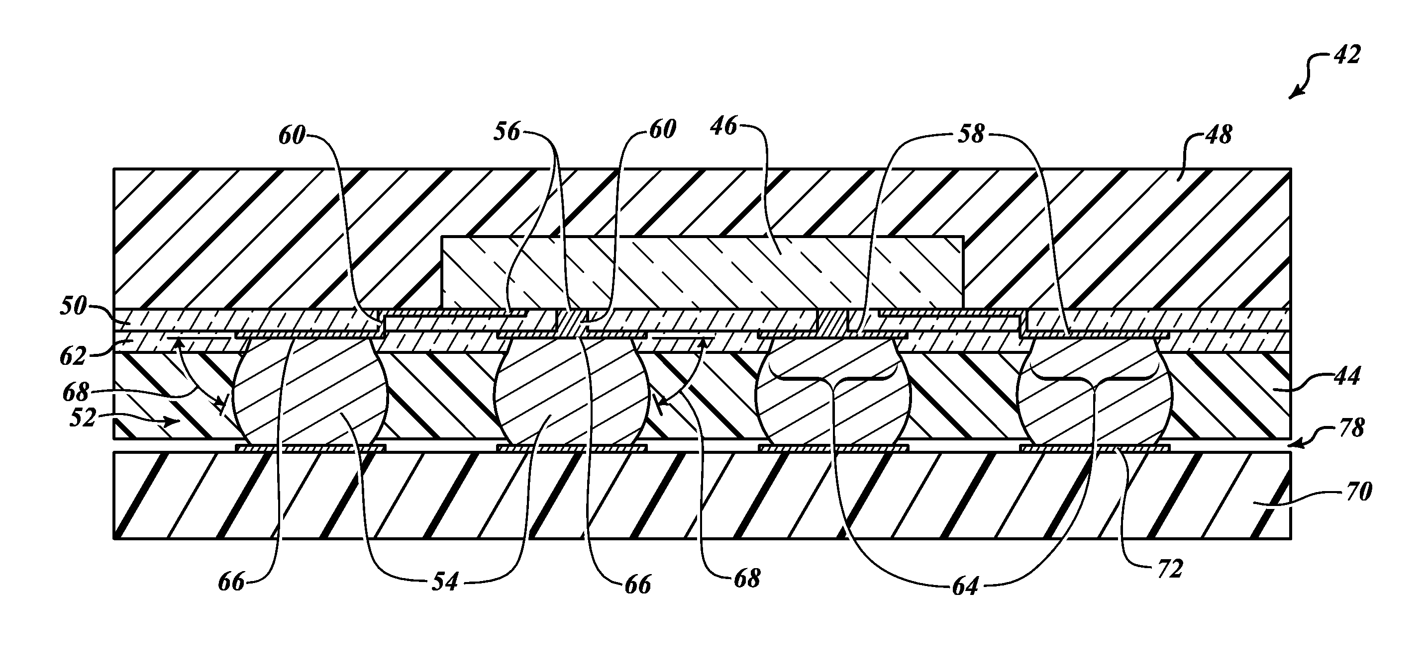
[0023]FIG. 7 illustrates an electronic package 42 having a polymeric layer 44 in accordance with principles of the present invention. For purposes of description, the polymeric layer 44 is described with reference to its application in a fan-out wafer-level electronic package. However, this in no way limits the use or application of the polymeric layer 44 to only fan-out wafer-level electronic packages. In fact, the polymeric layer 44 can be used or applied in other electronic packaging techniques including, for example, wafer-level chip scale packages, through-silicon via wafer-level packages, and electronic packaging techniques that use ball grid arrays (BGA) as an electrical interface.

[0024]In one embodiment, the package 42 includes the polymeric layer 44, a silicon die 46, an encapsulation material 48, a redistribution layer 50, and a solder ball array 52, including individual solder balls 54. The silicon die 46 includes electrical connection pads 56 on the die. The redistributi...


PUM

PropertyMeasurementUnit
Thicknessaaaaaaaaaa
Electrical conductoraaaaaaaaaa
Mechanical propertiesaaaaaaaaaa

Abstract

A polymeric layer encompassing the solder elements of a ball grid array in an electronics package. The polymeric layer reinforces the solder bond at the solder ball-component interface by encasing the elements of the ball grid array in a rigid polymer layer that is adhered to the package structure. Stress applied to the package through the ball grid array is transmitted to the package structure through the polymeric layer, bypassing the solder joint and improving mechanical and electrical circuit reliability. In one embodiment of a method for making the polymeric layer, solder elements bonded to external pads on a structure of the package are submerged in a fluidic form of the polymeric layer. The fluidic form is solidified and then a portion of the resulting polymeric layer is removed to make the solder elements accessible for mounting the package to a printed circuit board or other external circuit.

Description

BACKGROUND[0001]1. Technical Field[0002]This description generally relates to the field of electronic packaging, and, in particular, to mechanical components of electronic packages.[0003]2. Description of the Related Art[0004]Issues of mechanical and electrical reliability are of growing interest in ball bonded wafer-level packages, especially as the size of wafer-level packages increases. Larger package sizes increase the likelihood of mechanical failures, particularly at or near solder joints, from either externally applied mechanical stress or developed stress due to thermal expansion. Mechanical failures often lead to electrical failures.[0005]One common mechanical failure mode in wafer-level packages is passivation or redistribution layer delamination. FIG. 1 shows an example of a delamination failure, exhibited by a delamination crack 10 in a passivation layer 12. The delamination crack 10 in FIG. 1 developed as a result of a series of controlled drops conducted as part of a d...

Claims


Application Information

Patent Timeline
IPC IPC(8): H05K7/00H05K1/00H01R43/00
CPCH01L21/563Y10T29/49117H01L23/3128H01L24/20H01L2224/04105H01L2224/221H01L2224/814H01L2924/01082H01L2924/3025H01L23/293H01L2924/0002H01L2224/12105H01L2224/16225H01L2924/10253H01L2224/16227H01L2224/80815H01L2224/804H01L2224/05571H01L2224/05008H01L2924/01033H01L2924/014H01L24/19H01L2224/03334H01L2224/08238H01L2224/80357H01L24/05H01L24/08H01L24/80H01L2224/0391H01L2224/0401H01L2924/00012H01L2924/00H01L2224/05552
Inventor GOH, KIM-YONG
Owner STMICROELECTRONICS PTE LTD
Why Eureka
Try Eureka