Optical waveguide modulator

a modulator and optical waveguide technology, applied in non-linear optics, instruments, optics, etc., can solve the problems of non-linear distortion of the modulation of the output optical signal in conventional mz modulators, and distortion products that are problematic for systems that transmit analog signals or multi-band transmission. , to achieve the effect of suppressing the noise of relative intensity

Active Publication Date: 2011-06-30
LUMENTUM OPERATIONS LLC
View PDF32 Cites 60 Cited by
  • Summary
  • Abstract
  • Description
  • Claims
  • Application Information

AI Technical Summary

Benefits of technology

[0022]Embodiments of the invention described herein eliminate several of the problems of conventional LINMODs, and some embodiments also have additional benefits such as the suppression of Relative Intensity Noise (RIN) from the light source. The frequency response matching problem is solved by utilizing a single electrode to modulate two or more MZI's in parallel. The electrode structure is designed to modulate a plurality of waveguides with modulation efficiencies that may be different, but track each other over a target frequency range. Pairs of waveguides may have matched modulation frequency response, or the modulation response in a pair of waveguides may be matched over a frequency range but lowered by some ratio in comparison to another pair of waveguides. Some of the embodiments are directed to differential detection in order to cancel out laser RIN and / or CSO components. Exemplary topologies described hereinbelow allow for independent biasing of all constituent MZIs.
[0025]Another aspect of the present invention provides a waveguide modulator, comprising a substrate comprising electro-optical material, an optical input port formed on the substrate for receiving input light, first and second output ports formed on the substrate for outputting first and second output light, an optical splitting arrangement (OSA) formed in the substrate and optically coupled to the input port for splitting the input light into four light portions, an optical combining arrangement (OCA) formed in the substrate and optically coupled to the first and second output ports for forming the first and second output light from the four light portions, wherein the OSA is spaced apart from the OCA for defining therebetween a modulation section of the waveguide modulator, and first, second, third and fourth optical waveguides formed in the substrate and extending optically in parallel between the OSA and the OCA for guiding the four portions of light from the OSA to the OCA, with the second and third waveguides positioned in a space between the first and fourth waveguides. An RF signal electrode and one or more ground electrodes are disposed upon the substrate in the modulation section in the absence of other signal electrodes so as to induce an RF electrical field in each of the second and third waveguides when the RF electrode is connected to a source of RF electrical signal, wherein the one or more ground electrodes are disposed so as to shield the outer waveguides from the RF signal electrodes. The OSA comprises an optical beam combiner network for combining light from the first, second, and third waveguides into the first combined light, and for combining light from the second, third and fourth waveguides into the second combined light, so that light from each of the second and third waveguides is equally split between the first and second output ports. The waveguide modulator further comprises phase adjusting means for adjusting optical phases of light propagating in the first and forth waveguides, for adjusting an optical phase of light coupled from the second waveguide into the first output port, and for adjusting an optical phase of light coupled from the third waveguide into the second output port, so as to suppress third order modulation distortions in each of the first and second combined light and to effect a push-pull modulation of the first and second output light.

Problems solved by technology

One disadvantage of conventional voltage-controlled MZ structures is that its transmission characteristic, i.e. the dependence of an output optical power on the applied voltage, is substantially nonlinear, and is generally in the form of a sinusoid.
This non-linear MZ transmission characteristic of the MZ interferometer (MZI) structure results in non-linear distortions of the modulation of the output optical signal in conventional MZ modulators.
These distortion products are problematic for systems that transmit analog signals or multi-level digital signals that are analog in nature, such as Quadrature Amplitude Modulation (QAM) signals of various formats.
One disadvantage of the parallel LINMOD 10 is the loss of about half of the optical power due to the coupler having a coupling ratio that does not match the split ratio of the y-junction combiner near the output of the device.
One major problem with the prior art linearized modulators 10, 20 is the need for two separate, but identical RF electrodes being driven by outputs of an RF splitter.
In addition, separate cables and / or RE traces that route the RF signals to each of the signal electrodes may be slightly different in attenuation or length, causing differences in frequency response and / or phase response due to timing skew.
Any RF reflections that are not exactly matched will also result in ripple in the frequency response that is different for the two RF electrodes.
In practice, these difficulties can be overcome for modulation frequencies of less than 5 GHz, but become very difficult at frequencies approaching or above 20 GHz.
A major disadvantage of the LINMOD 30 for some applications is that the CSO components are not suppressed; in fact those components have about the same amplitude as the fundamental frequency components.
This device may not be suitable for multi-octave systems, where CSO suppression is required.
One drawback is that the ratio of optical power in the two polarizations must be carefully maintained to within a percent of target.
Another drawback is the need to bias light in two different polarizations.
The bias control of two polarizations adds complexity to the system.
Any polarization crosstalk after the modulator can seriously degrade CSO suppression.

Method used


Image

  • Optical waveguide modulator
  • Optical waveguide modulator
  • Optical waveguide modulator

Examples


Embodiment Construction

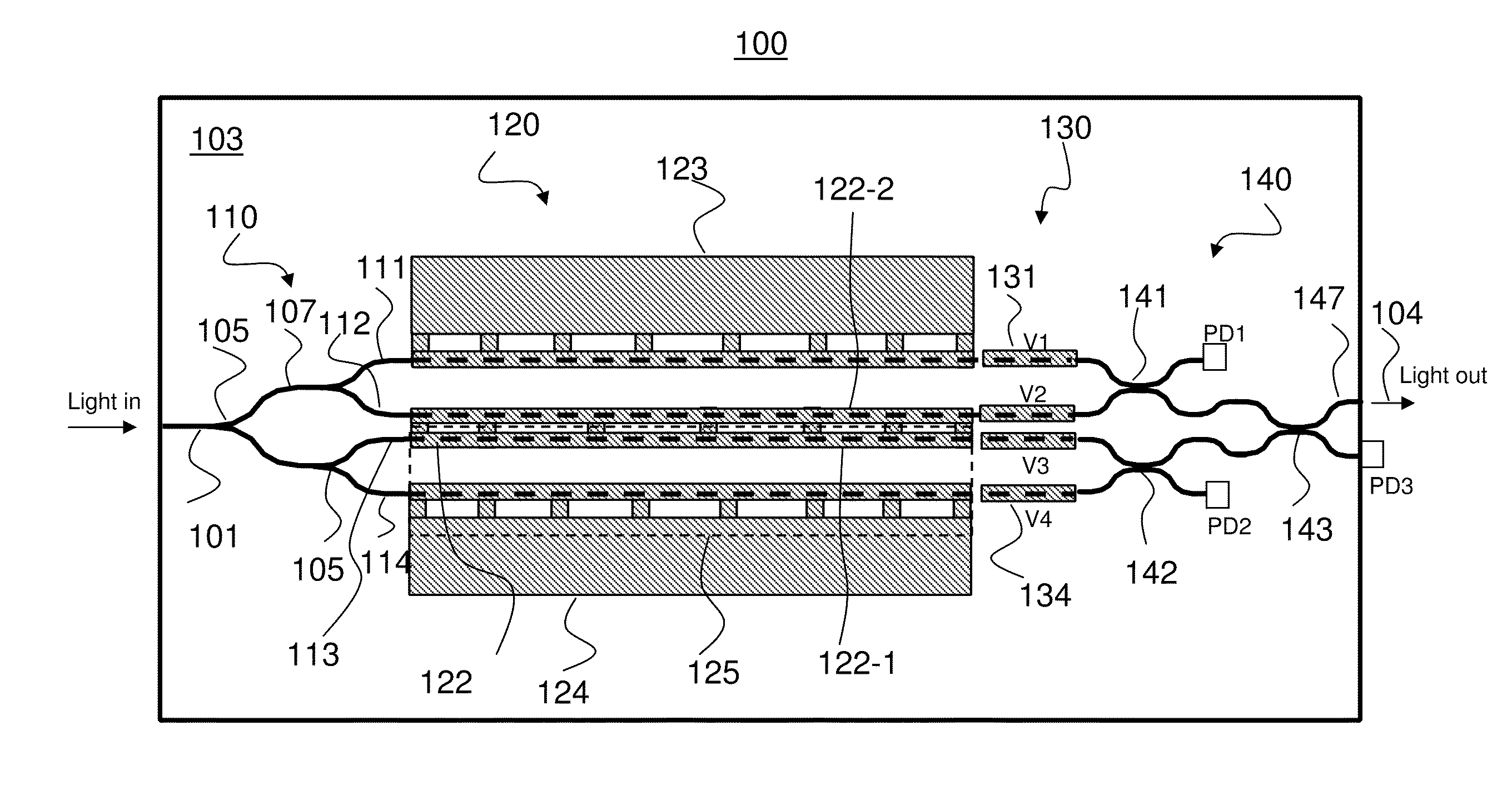
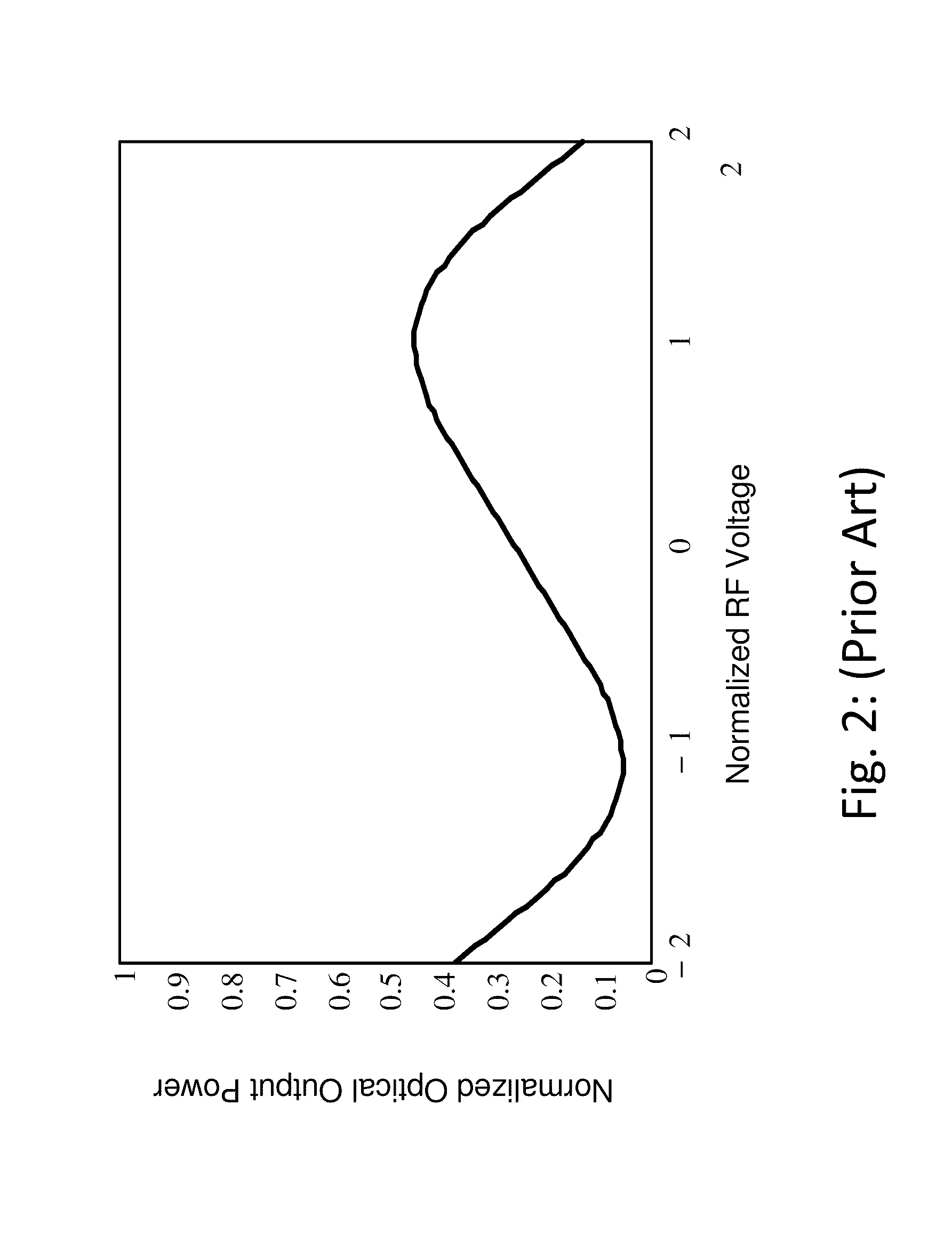
[0060]With reference to FIG. 9, there is illustrated a waveguide modulator 100 according to a first exemplary embodiment of the invention. FIG. 10 shows the transfer curve for the device. Note that the highest value in the transfer curve is about 0.5, indicating about 3 dB of optical penalty. The modulator 100 includes a modulation section 120 sandwiched between an input optical splitting arrangement (OSA) 110 for splitting input light launched in an input waveguide 101 into four light portions, and an optical combining arrangement (OCA) 140 for combining the four light portions into output light that exits the modulator 100 from an output waveguide 147, all formed in or upon a substrate 103 of an electro-optic material which refractive index is sensitive to a vertical electrical field that is normal to the plane of the substrate, such as a z-cut LiNbO3 (LN). Technologies for forming optical waveguides in LiNbO3 are well known in the art and will not be described herein. The modulat...


PUM

PropertyMeasurementUnit
modulation strengthaaaaaaaaaa
modulation strengthsaaaaaaaaaa
electrical fieldaaaaaaaaaa

Abstract

The invention relates to waveguide optical modulators wherein two or more waveguides are modulated with specific modulation strengths using a single straight signal electrode or a single multi-segment signal electrode. Modulation strengths for each of a plurality of waveguides modulated by a single multi-segment electrode are matched over a wide modulation frequency range. Linearized output characteristics with respect to second and third order distortions arc achieved in one aspect of the invention.

Description

CROSS-REFERENCE TO RELATED APPLICATIONS[0001]The present invention claims priority from U.S. Provisional Patent Application No. 61 / 291,252 filed Dec. 30, 2009, which is incorporated herein by reference. It is related to U.S. patent application Ser. No. 12 / 241,570 filed Sep. 30, 2008 and entitled “External Optical Modulator With Domain Inversion For Providing Constant Chirp Versus Frequency”, which claims priority from U.S. Provisional Patent Application No. 60 / 977,183 filed Oct. 3, 2007, both of which are incorporated herein by reference.TECHNICAL FIELD[0002]The present invention generally relates to optical waveguide modulators, and more particularly relates to linearized microwave optical waveguide modulators with a single RF signal electrode in at least a one modulation section thereof.BACKGROUND OF THE INVENTION[0003]Waveguide optical modulators are well known in the art and are used in a variety of applications. For high bandwidth application, for example at modulation rates in...

Claims


Application Information

Patent Timeline
Patent Type & Authority Applications(United States)
IPC IPC(8): G02F1/035
CPCG02F2203/19G02F1/225
Inventor KISSA, KARLMCBRIEN, GREGORY J.
Owner LUMENTUM OPERATIONS LLC
Why Eureka
Try Eureka