Method for Sealing Pores at Surface of Dielectric Layer by UV Light-Assisted CVD

a dielectric layer and light-assisted technology, applied in the direction of liquid surface applicators, pretreated surfaces, coatings, etc., can solve the problems of difficult control of film thickness to a range of 1 to several nm, poor coverage of height gaps, and rise in dielectric constant, etc., to achieve excellent controllability of film thickness, poor coverage of height gaps, and low throughput

Inactive Publication Date: 2011-06-30
ASM JAPAN
View PDF6 Cites 435 Cited by
  • Summary
  • Abstract
  • Description
  • Claims
  • Application Information

AI Technical Summary

Benefits of technology

In general, a damaged layer has lost carbon in the film and become hydrophilic, and can therefore cause the dielectric constant to rise if moisture is absorbed later on. This necessitates a repair process comprising, for example, removing absorbed moisture and adding CHx to the damaged areas to make the film hydrophobic in those areas. Also, a step to form a protective film is required after the repair process in order to protect the side walls of the low-k film against damage in the subsequent steps. This protective film must be resistant to plasma and chemical solutions and able to protect porous low-k films with a film thickness of 1 to several nm, and is generally formed via the PECVD or ALD technology. The PECVD process generally allows a film to form quickly, but controlling the film thickness to a range of 1 to several nm is difficult and coverage of height gaps is also poor. On the other hand, the ALD process provides excellent controllability of film thickness and coverage of height gaps, but formation of film is slow and the throughput is low. ALD is also disadvantageous in terms of cost because it requires expensive apparatuses.

Problems solved by technology

In general, a damaged layer has lost carbon in the film and become hydrophilic, and can therefore cause the dielectric constant to rise if moisture is absorbed later on.
The PECVD process generally allows a film to form quickly, but controlling the film thickness to a range of 1 to several nm is difficult and coverage of height gaps is also poor.
On the other hand, the ALD process provides excellent controllability of film thickness and coverage of height gaps, but formation of film is slow and the throughput is low.
ALD is also disadvantageous in terms of cost because it requires expensive apparatuses.

Method used


Image

  • Method for Sealing Pores at Surface of Dielectric Layer by UV Light-Assisted CVD
  • Method for Sealing Pores at Surface of Dielectric Layer by UV Light-Assisted CVD
  • Method for Sealing Pores at Surface of Dielectric Layer by UV Light-Assisted CVD

Examples


example 1

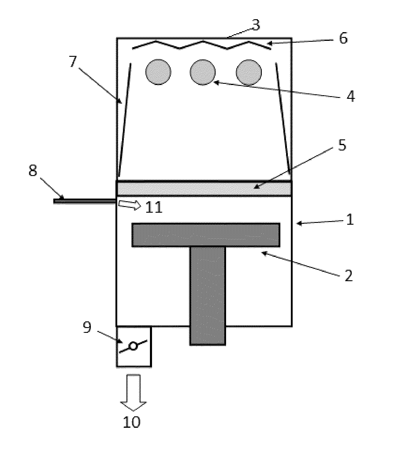
In this example, the apparatus shown in the schematic diagram of FIG. 1 was used to form a film.

As shown in FIG. 1, the UV irradiation apparatus used in this example comprises a UV lamp unit 3, UV irradiation window 5, vacuum reactor 1, heater table 2, process gas inlet tube 8, process gas inlet port 11, vacuum pump 10, and pressure control valve 9. The UV lamp unit 3 has UV mirrors 6, 7 for efficient irradiation of UV light. Note that multiple process gas inlet ports may be provided at roughly an equal pitch along the inner periphery walls of the reactor to allow gas to be introduced toward the center from the inner periphery walls of the reactor.

Note that the present invention is not at all limited to the apparatus shown in this figure and any other apparatus can be used so long as it can irradiate UV light. The apparatus shown comprises a chamber that can be controlled to pressures from vacuum to around atmospheric pressure, and a UV irradiation unit provided on top of the chambe...

example 2

According to the procedures and conditions used in Example 1, substrates having a porous layer (ELK film) were prepared, on which the following treatments were conducted, respectively:

1) Oxygen Plasma Treatment:

The ELK film was exposed to an oxygen plasma for 20 sec, which was generated by an RF power (13.56 MHz, 50 W) applied to oxygen-supplying gas (O2, 7 sccm) at a temperature of 250° C. at a pressure of 3.5 Torr.

2) Uv Restoration:

According to the procedures and conditions used in Example 1, the oxygen plasma treated ELK film obtained in 1) was subjected to UV restoration treatment where the temperature of the heating table was 300° C., the pressure was 10 Ton, nitrogen gas (500 sccm) and hydrocarbon gas (butadiene, 90 sccm) were introduced, and the substrate was irradiated with UV light for 4 minutes.

3) Thermal Annealing:

The oxygen plasma treated ELK film obtained in 1) was annealed at a temperature of 300° C. for five minutes in an atmosphere of nitrogen at a pressure of 5 Torr...


PUM

PropertyMeasurementUnit
depthaaaaaaaaaa
thicknessaaaaaaaaaa
wavelengthaaaaaaaaaa

Abstract

A method for sealing pores at a surface of a dielectric layer formed on a substrate, includes: providing a substrate on which a dielectric layer having a porous surface is formed as an outermost layer; placing the substrate in an evacuatable chamber; irradiating the substrate with UV light in an atmosphere of hydrocarbon and/or oxy-hydrocarbon gas; sealing pores at the porous surface of the dielectric layer as a result of the irradiation; and continuously irradiating the substrate with UV light in the atmosphere of hydrocarbon and/or oxy-hydrocarbon gas until a protective film having a desired thickness is formed on the dielectric layer as a result of the irradiation.

Description

BACKGROUND1. Field of the InventionThe present invention generally relates to restoration of damage caused to a porous low-k film by ILD patterning steps, such as resist ashing, plasma cleaning, etc.2. Description of the Related ArtAs the device design rule has been reduced, dielectric constants of inter-layer insulation films continue to fall and 32-nm generation and newer devices are now achieving dielectric constants of less than 2.5. As the dielectric constants of dielectric films (low-dielectric-constant films, or “low-k films”) fall, however, porosities are increasing and consequently the trend for lower dielectric constants is giving rise to problems resulting from higher porosities of inter-layer insulation films, such as lower resistance to plasma and chemical solutions and diffusion of barrier metal into the film. Since low-k films are exposed to chemicals during etching, resist ashing, wet cleaning and other steps in the wire machining process, insufficient resistance to ...

Claims


Application Information

Patent Timeline
Patent Type & Authority Applications(United States)
IPC IPC(8): C08J7/18
CPCB05D1/60B05D3/061B05D7/22H01L21/02126H01L21/02167H01L21/76831H01L21/3105H01L21/67115H01L21/76825H01L21/76826H01L21/02203
Inventor MATSUSHITA, KIYOHIROKIMURA, YOSUKEYANAGISAWA, IPPEI
Owner ASM JAPAN
Why Eureka
Try Eureka