Layered semiconductor neutron detectors

a neutron detector and semiconductor technology, applied in the direction of material analysis, measurement with semiconductor devices, instruments, etc., can solve the problems of incomplete charge collection, low temperature operation of ge-based gamma-ray detectors, and high density of czt trapping centers

Active Publication Date: 2011-07-07
RGT UNIV OF CALIFORNIA
View PDF11 Cites 34 Cited by
  • Summary
  • Abstract
  • Description
  • Claims
  • Application Information

AI Technical Summary

Benefits of technology

[0018]Embodiments of the present invention provide room temperature operating solid state hand held neutron detectors. Detectors in accordance with the present invention integrate one or more relatively thin layers or micro- or nano-structure arrays incorporating a high neutron interaction cross-section element with semiconductor detectors. The high neutron interaction cross-section element (e.g., Gd, B or Li) incorporating layer(s) or array(s) can be elemental, alloys, organics, or doped semiconductors and can be in the form of unstructured layers or micro- or nano-structured arrays. Such architecture provides high efficiency neutron detector devices by capturing substantially more carriers produced from high energy particles generated by neutron interaction, and are not limited by the asymmetry of semiconductor materials' mobility-lifetime products for electrons and holes.

Problems solved by technology

A major drawback, due to the small band gap of germanium, is that Ge-based gamma-ray detectors have to be operated at low temperature.
However, the problem with most high-Z semiconductors is the high probability of charge trapping which, depending on the position of the interaction between the electrodes, leads to incomplete charge collection.
CZT on the other hand has a much higher density of trapping centers due to defects.
In the output spectrum this gives rise to serious spectral distortion.
Although there are a number of techniques developed to correct or compensate for this trapping effect, the performance of CZT detectors has not yet reached the level of which it is theoretically capable due to material quality and is still far from that of Ge detectors.
However, neutrons only interact weakly with most known semiconductor detector materials.
However, unlike gamma-ray detection where semiconductor detectors based on Ge and CdZnTe are available, no comparable semiconductor neutron detector materials have been developed.
For gamma-ray detectors, unlike silicon or gallium arsenide, it is very difficult to grow large size single crystals of CZT, which have been made traditionally from crystals that are grown by a high pressure method.
While the high pressure method yields quality detectors, the crystal uniformity is limited and the detector yield is low.
Other than a few variations of the high pressure crystal growth method, there have been no reports of effective alternatives to grow high quality crystalline semiconductor materials for radiation detectors.
Incomplete charge collection, due to poor charge transport properties of the detector materials, degrades the energy resolution and lowers the effective photo peak efficiency for gamma-rays as well as for neutrons.
The relatively low hole mobility and life time cause hole trapping and consequent loss in signal.
However, CdZnTe has the drawback of lower hole life time (τe=5 μs, τh=200 ns, μe=1350 cm2 / Vs and μh=120 cm2 / Vs).
However, its carrier lifetime is far from what needed to achieve good energy resolution.

Method used


Image

  • Layered semiconductor neutron detectors
  • Layered semiconductor neutron detectors
  • Layered semiconductor neutron detectors

Examples


Embodiment Construction

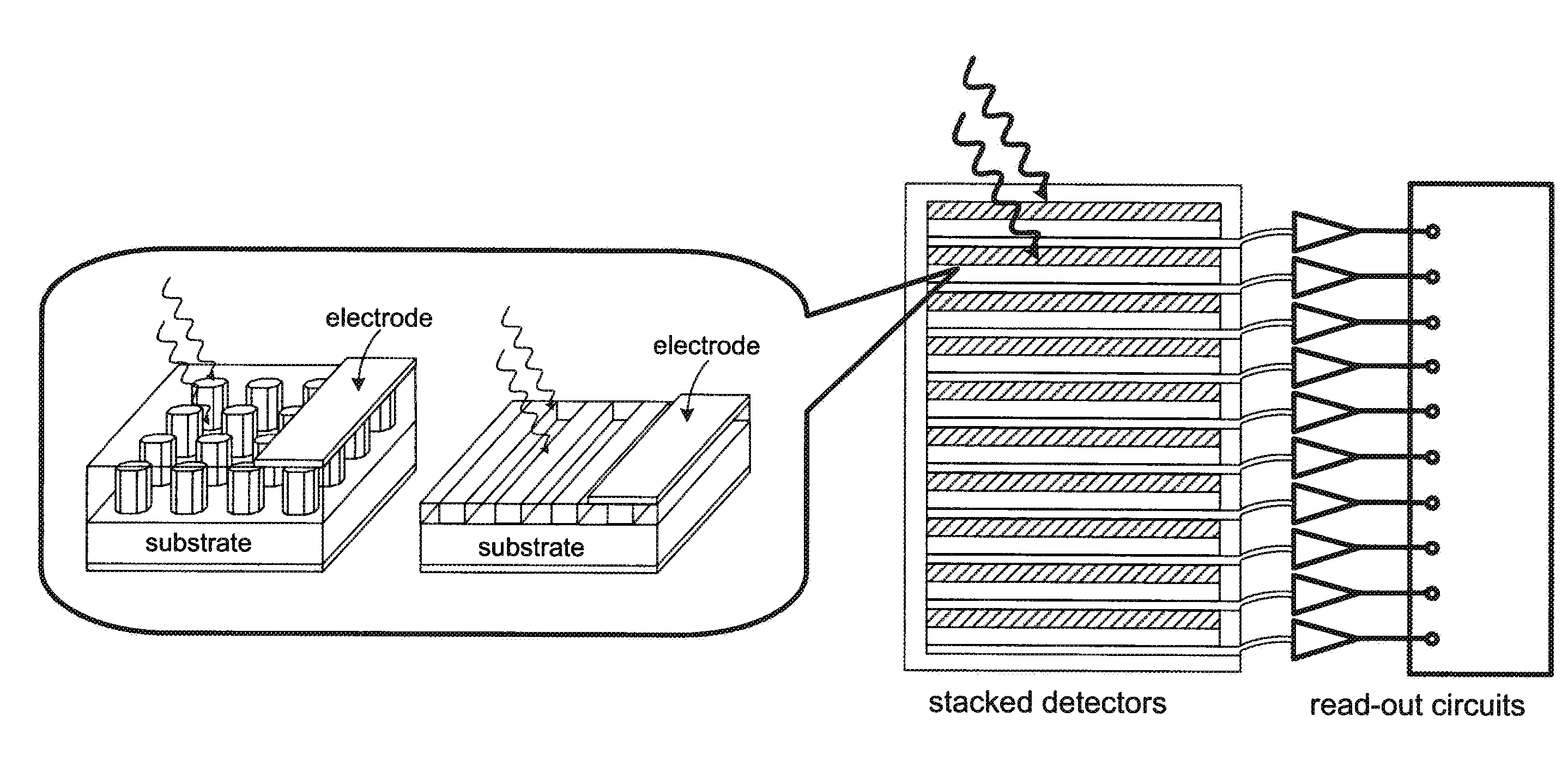
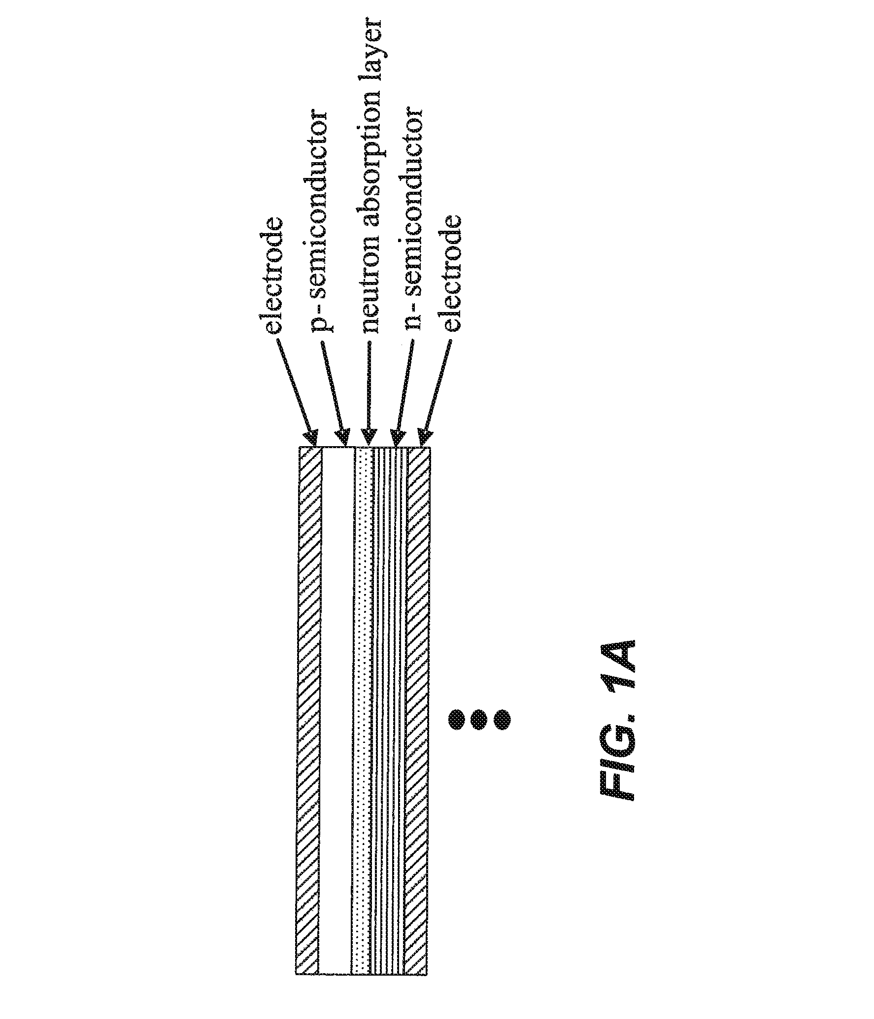
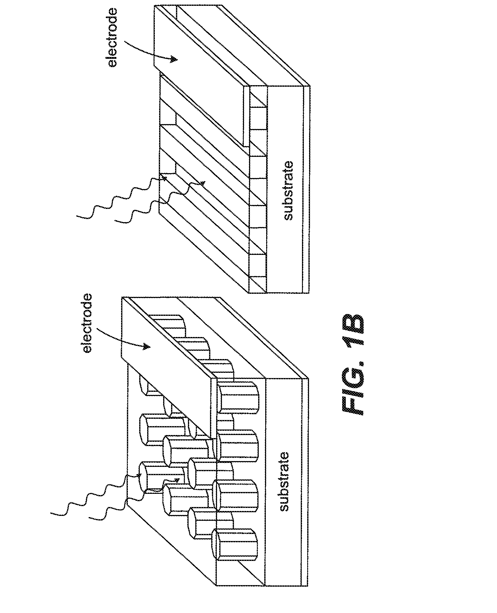
[0020]Reference will now be made in detail to specific embodiments of the invention. Examples of the specific embodiments are illustrated in the accompanying drawings. While the invention will be described in conjunction with these specific embodiments, it will be understood that it is not intended to limit the invention to such specific embodiments. On the contrary, it is intended to cover alternatives, modifications, and equivalents as may be included within the spirit and scope of the invention as defined by the appended claims. In the following description, numerous specific details are set forth in order to provide a thorough understanding of the present invention. The present invention may be practiced without some or all of these specific details. In other instances, well known process operations have not been described in detail so as to not unnecessarily obscure the present invention.

[0021]Introduction

[0022]The invention relates to a new apparatus and techniques to improve ...


PUM


Abstract

Room temperature operating solid state hand held neutron detectors integrate one or more relatively thin layers of a high neutron interaction cross-section element or materials with semiconductor detectors. The high neutron interaction cross-section element (e.g., Gd, B or Li) or materials comprising at least one high neutron interaction cross-section element can be in the form of unstructured layers or micro- or nano-structured arrays. Such architecture provides high efficiency neutron detector devices by capturing substantially more carriers produced from high energy α-particles or γ-photons generated by neutron interaction.

Description

CROSS-REFERENCE TO RELATED APPLICATIONS[0001]This application claims priority to U.S. Provisional Patent Application No. 61 / 083,352, titled LAYERED SEMICONDUCTOR NEUTRON DETECTORS, filed Jul. 24, 2008, the disclosure of which is incorporated herein by reference in its entirety and for all purposes.STATEMENT OF GOVERNMENTAL SUPPORT[0002]The invention described and claimed herein was made at least in part utilizing funds supplied by the U.S. Department of Energy under Contract No. DE-AC02-05CH11231. The Government has certain rights in this invention.BACKGROUND OF THE INVENTION[0003]Semiconductor detectors are among the most widely used radiation detection devices. They have found applications ranging from space physics to medicine, to defense and homeland security. Semiconductor radiation detectors generally operate by absorbing a quantum of gamma-ray or a neutron and converting the radiation energy into a number of electron-hole pairs that is proportional to the absorbed energy. Aft...

Claims


Application Information

Patent Timeline
Patent Type & Authority Applications(United States)
IPC IPC(8): G01T3/08H01L31/115H01L31/18
CPCG01T3/08
Inventor MAO, SAMUEL S.PERRY, DALE L.
Owner RGT UNIV OF CALIFORNIA
Why Eureka
Try Eureka