Superfilled metal contact vias for semiconductor devices

a metal contact via and semiconductor technology, applied in semiconductor devices, semiconductor/solid-state device details, electrical equipment, etc., can solve the problems of difficult to adequately control a process and less desirable tungsten than

Active Publication Date: 2011-07-07
GLOBALFOUNDRIES US INC
View PDF13 Cites 77 Cited by
  • Summary
  • Abstract
  • Description
  • Claims
  • Application Information

AI Technical Summary

Benefits of technology

[0016]In one embodiment, the electroplating step can be performed without forming a void within the contact opening.

Problems solved by technology

It can be difficult to adequately control a process to form the required liners and a capping layer to encase the copper within openings.
However, the increasingly small size of contact vias make tungsten less desirable than before.

Method used


Image

  • Superfilled metal contact vias for semiconductor devices
  • Superfilled metal contact vias for semiconductor devices
  • Superfilled metal contact vias for semiconductor devices

Examples


Embodiment Construction

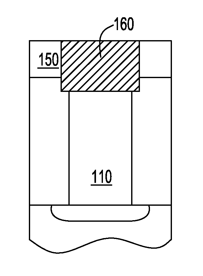
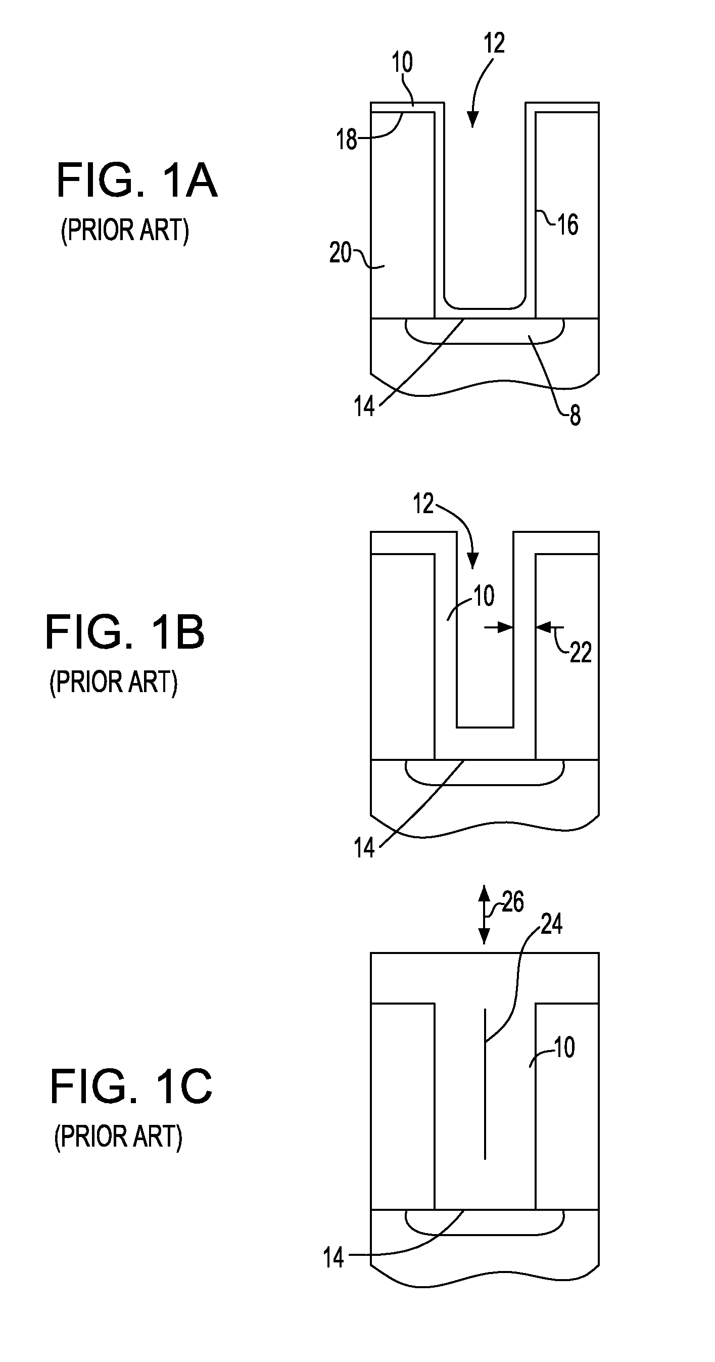
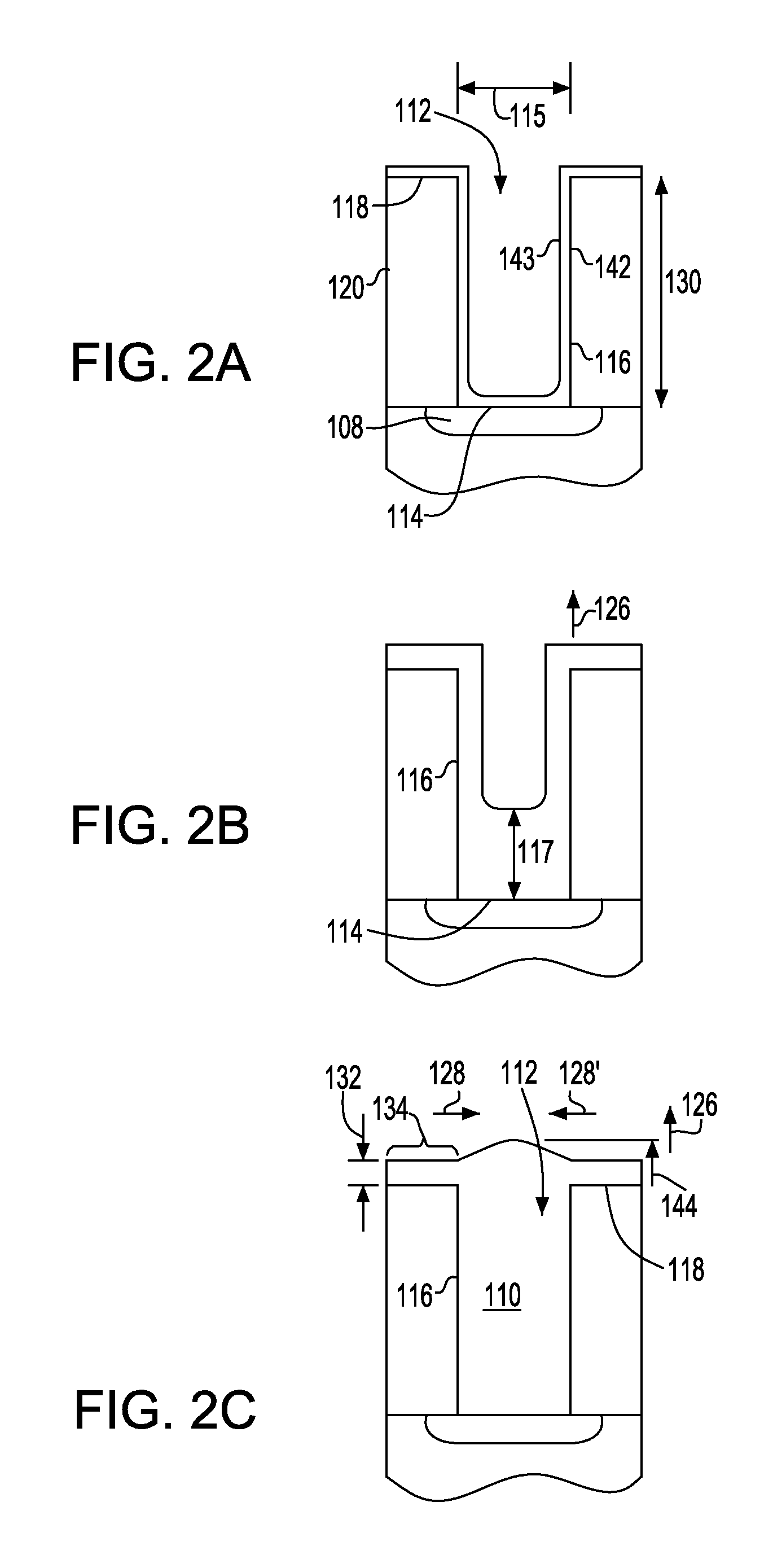
[0032]The inventors have recognized that seams and voids within contact vias, if they remain unaddressed, could pose significant problems for conductive interconnects in current or future semiconductor technology generations. Seams or voids can increase the electrical resistance of contact vias, leading to degraded device performance. Conductivity and reliability of the contact vias could be more severely impacted because future contact vias have smaller widths. At the same time, the volume occupied by the seam and voids that can occur at the seam are not expected to decrease. The net result of the seam on future contact vias is that seams and voids could occupy a proportionately greater amount of the total volume within contact vias. This result should be avoided, if possible, by use of a metal filling process which is better able to avoid forming a seam when filling a contact via, and which reduces the likelihood that voids will occur. Particularly, seams and voids should be avoid...


PUM

PropertyMeasurementUnit
widthaaaaaaaaaa
diameteraaaaaaaaaa
diameteraaaaaaaaaa

Abstract

In accordance with one aspect of the invention, a method is provided for fabricating a semiconductor element having a contact via. In such method, a hole can be formed in a dielectric layer to at least partially expose a region including at least one of semiconductor or conductive material. A seed layer can be deposited over a major surface of the dielectric layer and over a surface within the hole. In one embodiment, the seed layer can include a metal selected from the group consisting of iridium, osmium, palladium, platinum, rhodium, and ruthenium. A layer consisting essentially of cobalt can be electroplated over the seed layer within the hole to form a contact via in electrically conductive communication with the region.

Description

BACKGROUND OF THE INVENTION[0001]1. Field of the Invention[0002]The present invention relates to semiconductor devices and their manufacture, and more specifically to semiconductor devices having metal vias and their manufacture.[0003]2. Description of the Related Art[0004]A typical semiconductor chip includes active devices such as transistors and wiring referred to as conductive interconnects that connect the transistors together in form of an integrated circuit to perform the function of the chip. In general, with each generation of semiconductor chips, the sizes of transistors and conductive interconnect becomes smaller, mostly to provide a greater number of transistors (and function) for the size of the chip being made.[0005]Semiconductor chips typically have an active semiconductor device area which is adjacent to a top or major surface of the chip. The active area typically is disposed in horizontal directions which run parallel with the top surface. The conductive interconne...

Claims


Application Information

Patent Timeline
Patent Type & Authority Applications(United States)
IPC IPC(8): H01L23/48H01L21/768
CPCH01L21/2885H01L21/76843H01L21/76873H01L21/76877H01L23/485H01L2924/0002H01L23/53266H01L2924/00
Inventor KELLY, JAMES J.BASKER, VEERAGHAVAN S.HARAN, BALA S.SEO, SOON-CHEONVO, TUAN A.
Owner GLOBALFOUNDRIES US INC
Why Eureka
Try Eureka