Configuration of a multilevel flash memory device

a memory device and multi-level technology, applied in the direction of memory address/allocation/relocation, program control, instruments, etc., can solve the problems of reducing performance, affecting the performance of memory devices, and many specific parameters of operation such as the timing of certain phases of operation, so as to simplify and speed up the trimming operation of the device

a memory device and multi-level technology, applied in the direction of memory address/allocation/relocation, program control, instruments, etc., can solve the problems of reducing performance, affecting the performance of memory devices, and many specific parameters of operation such as the timing of certain phases of operation, so as to simplify and speed up the trimming operation of the device

US20110167206A1Active Publication Date: 2011-07-07MICRON TECH INC

Image

  • Configuration of a multilevel flash memory device
  • Configuration of a multilevel flash memory device
  • Configuration of a multilevel flash memory device

Examples


Embodiment Construction

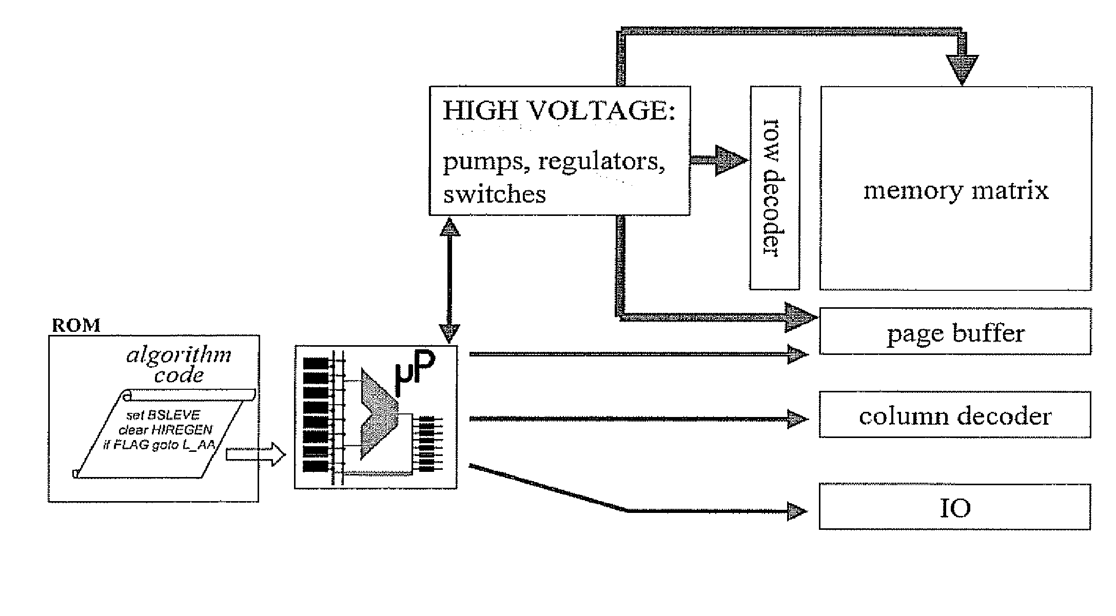
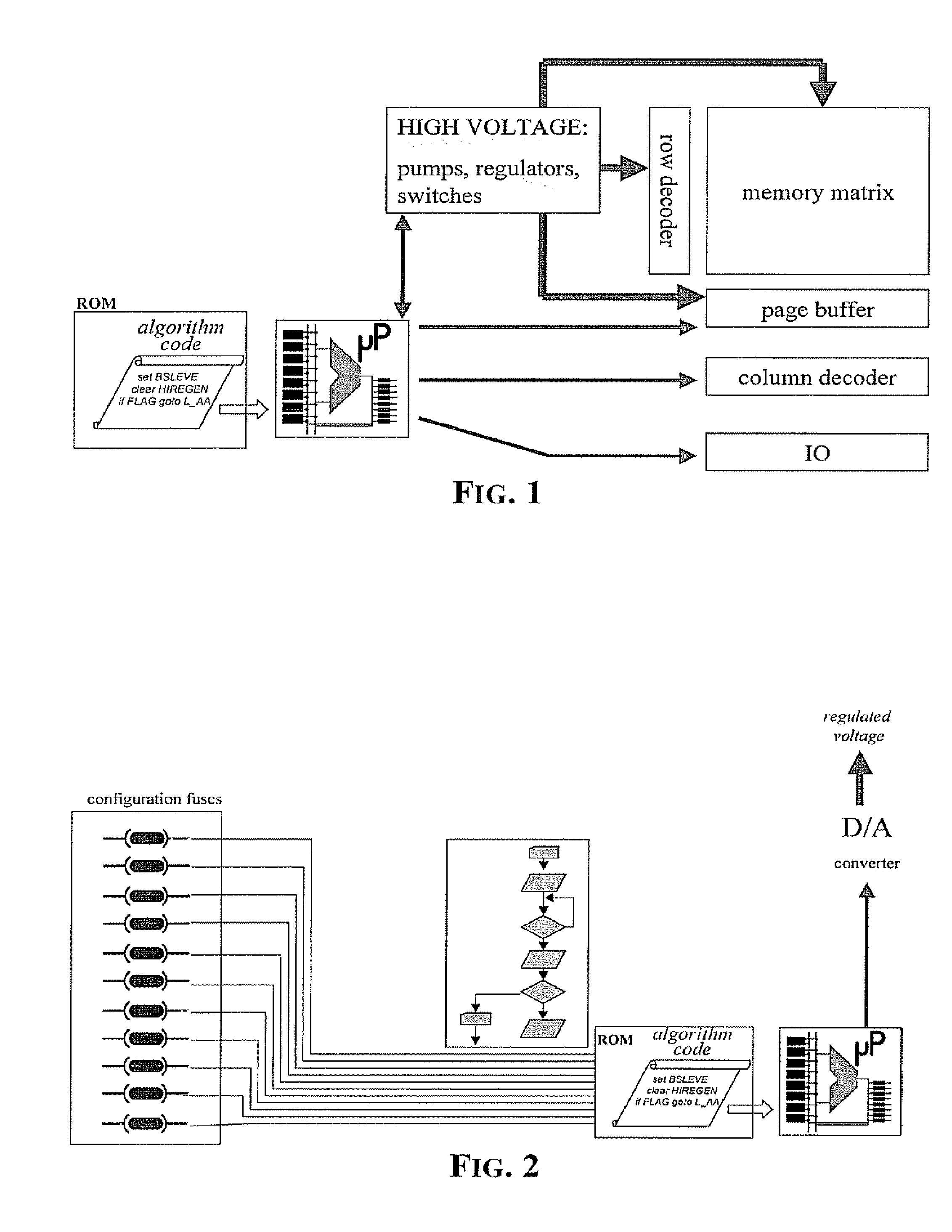
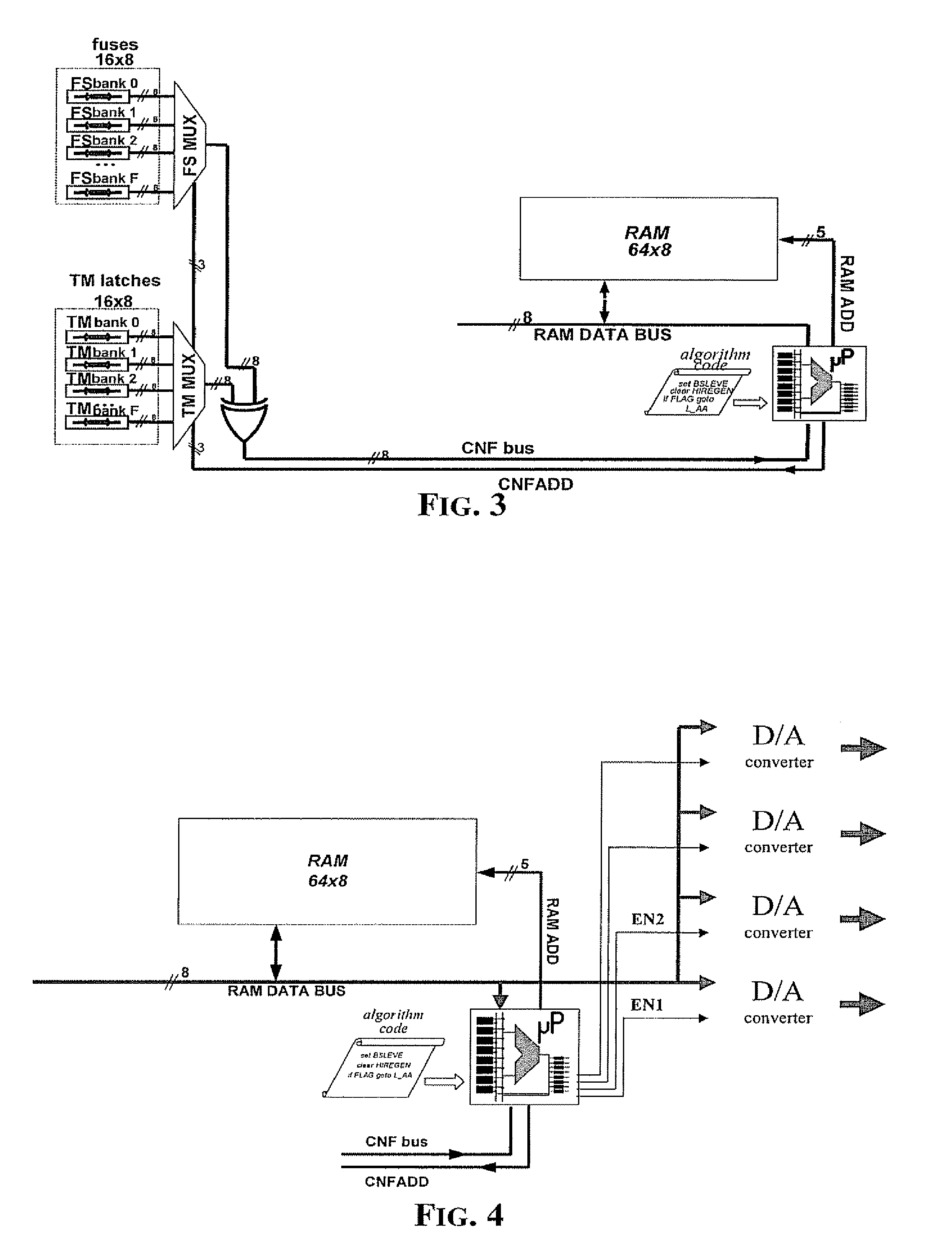
FIG. 3 illustrates the hardware elements of a multi-level NAND flash memory device with an embedded micro-controller of the present invention that are involved in the execution of a specific power-on algorithm code at every power-on of the device for processing and storing in the ancillary random access memory of configuration data. At every power-on of the device, once the supply voltage has reached a level sufficient to ensure the correct functioning of all logic circuits, a specific algorithm of power-on is executed by the micro-controller μP.

During this phase, the micro-controller μP addresses the plurality of configuration fuses FUSES 16×8, through the address bus CNF-ADD, and reads the relative configuration bit content of the fuses from the CNF-BUS. The information acquired from the configuration fuses of the device is processed into a form more readily usable (algorithm-friendly form) by the control algorithms that are executed during the various operation phases of the memo...


PUM


Abstract

A multi-level flash memory device allows for a faster and more effective configuration of the operating parameters of the memory device for performing the different functioning algorithms of the memory. The identification of an optimal configuration of the operating parameters of the memory device during testing is simplified by allowing for a one-time processing of configuration bits into algorithm-friendly data that are stored in an embedded ancillary random access memory at every power-on of the memory device. This is done by executing a specific power-on algorithm code stored in the ancillary read only memory of the embedded microprocessor.

Description

FIELD OF THE INVENTIONThe present invention relates to non-volatile memory devices, and more particularly, to multi-level flash memory devices embedded in a microcontroller for executing algorithm codes stored in a read only memory.BACKGROUND OF THE INVENTIONMulti-level flash memory devices of NAND architecture are in an initial phase of development. This implies that many specific parameters of operation such as the timing of certain phases of operation, biasing voltages and the like cannot be optimally defined in the design stage before gathering clear responses from the silicon.Therefore, in the development phase of the design of a new memory device, it is necessary to carry out the control algorithms of operation of the memory device with a sufficiently ample possibility of varying the operating parameters. All the possible alternatives of configuration should be selectable in the device in a definitive or permanent manner and / or in a test mode (non-permanent) manner in order to...

Claims


Application Information

Patent Timeline
07 Jul 2011
Publication
US20110167206A1
IPC
G06F12/02
CPC
G11C16/20; G11C11/5621
Inventors
BOVINO, ANGELO; RAVASIO, ROBERTO