Semiconductor device and semiconductor device manufacturing method

a semiconductor device and semiconductor technology, applied in the direction of semiconductor devices, semiconductor/solid-state device details, electrical apparatus, etc., can solve the problems that the semiconductor wafer may be impossible to handle, and achieve the effect of reducing compressive stress of each first dielectric film, and effectively inhibiting warping deformation

Active Publication Date: 2011-07-21
ROHM CO LTD
View PDF15 Cites 36 Cited by
  • Summary
  • Abstract
  • Description
  • Claims
  • Application Information

AI Technical Summary

Benefits of technology

[0034]The vias may be made of a metallic material containing Cu, and in this case, the second dielectric film is preferably made of a material having a barrier property against Cu. Cu contained in the vias can be prevented from diffusing into the first dielectric films formed on the vias, due to the second dielectric film.
[0035]The first wire may be made of a metallic material containing Cu, and in this case, the semiconductor device preferably further includes a barrier film, interposed between the interlayer dielectric film and the first wire, made of a material having a barrier property against Cu. Cu contained in the first wire can be prevented from diffusing into the interlayer dielectric film, due to the barrier film.
[0036]The barrier film preferably has tensile stress. Compressive stress of the compressive stress films of the interlayer dielectric film can be canceled, due to the tensile stress of the barrier film. Consequently, the semiconductor substrate can be more effectively inhibited from causing warping deformation.
[0037]The vias are preferably formed by a single damascene process. In the single damascene process, a step of forming a via in a first dielectric film is separately carried out every first dielectric film, and selective etching and planarization of the first dielectric film are performed in each step. Therefore, the compressive stress of each first dielectric film can be reduced. Consequently, the semiconductor substrate can be effectively inhibited from causing warping deformation.

Problems solved by technology

If a matrix for the semiconductor substrate is a semiconductor wafer having a diameter of 300 mm, particularly remarkable warping deformation may be caused, and the semiconductor wafer may be impossible to handle.

Method used


Image

  • Semiconductor device and semiconductor device manufacturing method
  • Semiconductor device and semiconductor device manufacturing method
  • Semiconductor device and semiconductor device manufacturing method

Examples


Embodiment Construction

[0057]Embodiments of the present invention are now described in detail with reference to the attached drawings.

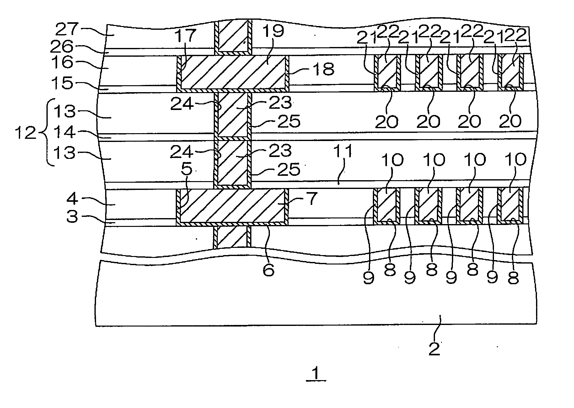
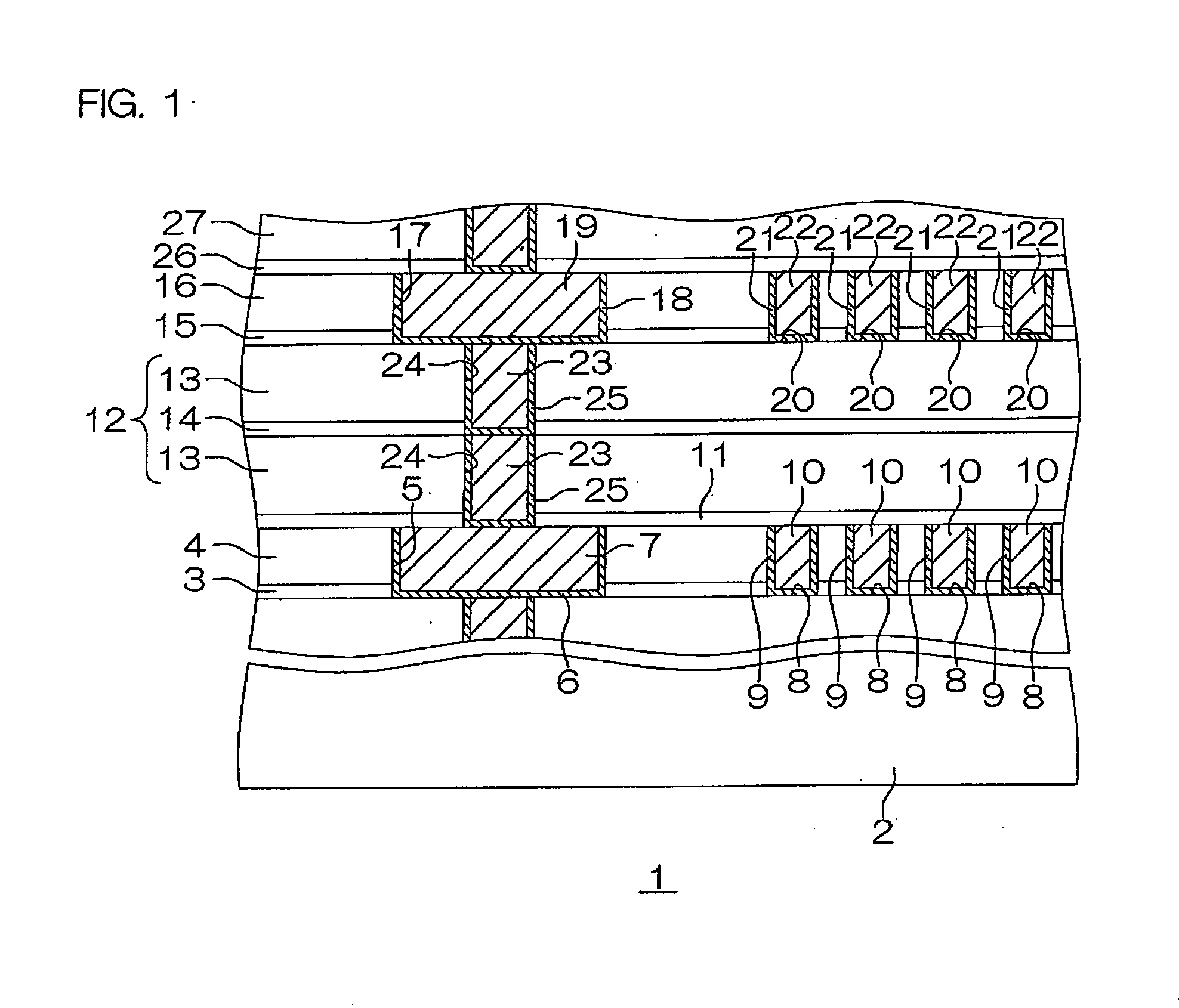
[0058]FIG. 1 is a schematic sectional view of a semiconductor device according to an embodiment of the present invention.

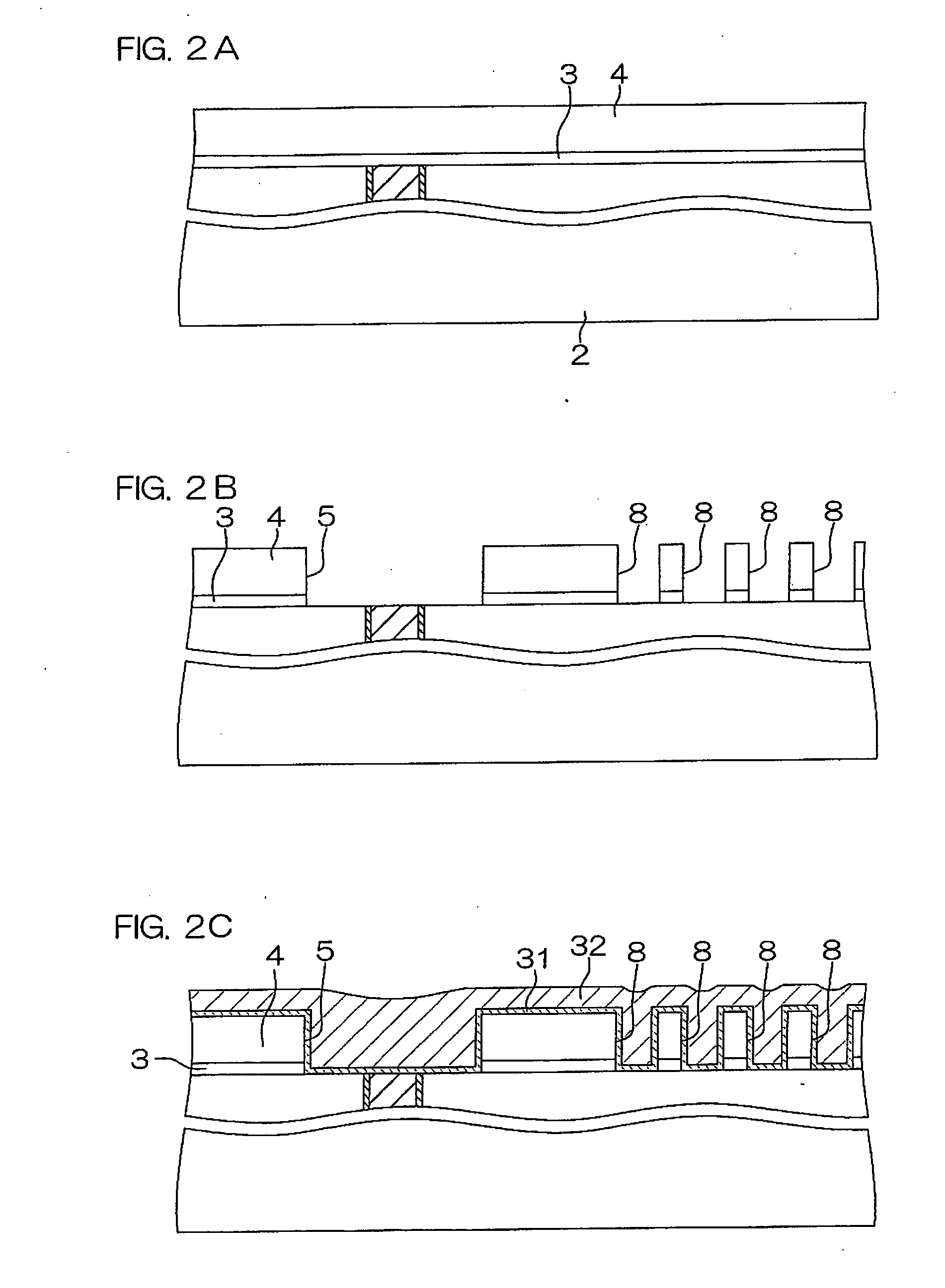
[0059]A semiconductor device 1 is a transformer device, and includes a semiconductor substrate 2. As the semiconductor substrate 2, an Si (silicon) substrate, an SiC (silicon carbide) substrate or the like can be illustrated.

[0060]An etching stopper film 3 is stacked on the semiconductor substrate 2. The etching stopper film 3 is made of SiN, and has tensile stress. The thickness of the etching stopper film 3 is 0.3 μm (=300 nm), for example.

[0061]A first wiring layer 4 is stacked on the etching stopper film 3. The first wiring layer 4 is made of SiO2, and has compressive stress. The thickness of the first wiring layer 4 is 2.1 μm, for example.

[0062]A first wiring trench 5 is formed in the first wiring layer 4. The first wiring trench 5 is in the form of ...


PUM

PropertyMeasurementUnit
dielectric breakdownaaaaaaaaaa
dielectric strengthaaaaaaaaaa
thicknessaaaaaaaaaa

Abstract

A semiconductor device according to the present invention includes a semiconductor substrate, and an interlayer dielectric film, formed on the semiconductor substrate, having a multilayer structure of a compressive stress film and a tensile stress film.

Description

TECHNICAL FIELD[0001]The present invention relates to a semiconductor device, particularly a power semiconductor device and a method of manufacturing the same.BACKGROUND ART[0002]In recent years, a power semiconductor device (hereinafter referred to as a “transformer device”) including a transformer has been developed in the field of power electronics.[0003]FIG. 5 is a schematic sectional view of a transformer device.[0004]A transformer device 101 includes a first wiring layer 102 made of SiO2 (silicon oxide) on an unshown semiconductor substrate.[0005]A first wiring trench 103 is formed in the first wiring layer 102. A first wire 105 made of a metallic material (hereinafter referred to as a “Cu wire material”) mainly composed of Cu (copper) is embedded in the first wiring trench 103 through a barrier metal 104. A coil groove 106, spiral in plan view, having the same depth as the first wiring trench 103 is formed in the first wiring layer 102 at an interval from the first wiring tre...

Claims


Application Information

Patent Timeline
Patent Type & Authority Applications(United States)
IPC IPC(8): H01L23/532H01L21/762
CPCH01L21/76801H01L21/76829H01L23/5227H01L23/53238H01L2924/0002H01L23/53295H01L2924/00
Inventor NAKAGAWA, RYOSUKE
Owner ROHM CO LTD
Why Eureka
Try Eureka