Method of manufacturing semiconductor memory

a semiconductor memory and manufacturing method technology, applied in the manufacture/treatment of semiconductor devices, electrical apparatus, electrical devices, etc., can solve the problems of difficult to achieve satisfactorily-reproducible fittings, difficult to perform partial insulation coatings or projection forming, and difficult to keep positional relationships consistent, so as to reduce the curvature radius and reduce the projection curvature. , the effect of small curvature radius

Active Publication Date: 2011-07-21
PANASONIC CORP
View PDF16 Cites 17 Cited by
  • Summary
  • Abstract
  • Description
  • Claims
  • Application Information

AI Technical Summary

Benefits of technology

In order to better obtain the advantageous effects of the projection such as the electric charge crowding effect, and so on, a smaller curvature radius of the projection is advantageous. In order to reduce the curvature radius with the method in Patent Reference 5, it is necessary to suppress the thickness of the electrode thin-plate which is the projection. Patent Reference 5 exemplifies a case where 20 nanometers is the thickness.
Next, the length of the projection shall be described. Since the CMP process used in Patent Reference 5 is a process requiring physical contact with the substrate of the pad in the fabrication, obtaining intra-plane uniformity and inter-wafer reproducibility is difficult. Normally, there is a variation in the tens of nanometers or more in the amount of etching. In view of this, in order to reliably form the projection across the entire region of all the wafers, the forming must be carried out with a higher elevation change in consideration of etching variation. As a result of when this method is used, the length (amount of projection) of the projection of the electrode necessarily becomes more than several tens of nanometers. In addition, the variation in the length of the projection is in the tens of nanometers. With such limitations, the projection that is formed using this method becomes longer than the projections formed using other methods, and variation becomes significant.
In the variable resistance memory, the electrical resistance change in a variable resistance layer or the interface of the variable its resistance layer and the electrode fulfills the role of information storage. Therefore, it is necessary to detect such resistance change in order to read information. Normally, resistance change is detected based on the amount of current flowing to the element or voltage drop that is measured by a circuit which uses a transistor, and the like. At is this time, the circuit can detect the resistance in the entire path from the variable resistance memory to the detection circuit. In other words, aside from the resistance of the variable resistance layer, it is possible to measure the resistance in the entire path from the variable resistance layer up to the measurement circuit such as a transistor. Therefore, no matter how large the resistance change at the part of the variable resistance layer is, if the resistance value at the fixed-resistance part in which the resistance throughout the entire path does not change is large, the resistance change percentage as a whole becomes small, and resistance change detection becomes difficult. Furthermore, if the resistance value of the fixed-resistance part varies in each element, it becomes difficult to distinguish between differences in resistance due to differences in memory information and variations in the resistance values of the fixed-resistance parts.
In the case of the thin-plate projection formed using the method in Patent Reference 5, the electrical resistance of the projection part is inversely proportional to the thickness of the thin-plate. Assuming that this thickness is several nanometers, the electrical resistance of this part cannot be disregarded. In particular, TiN, which is the conductive material disclosed in Patent Reference 5, has an electrical resistivity of approximately 10 to the −1 power to 0 power Ωm (ohm meters), and thus has a resistance that is approximately 1000 times to 10,000 times higher than Pt or Al.
For example, in the case where the projection is formed using TiN with a width of 50 nanometers and a thickness of 5 nanometers, even assuming that the electrical resistivity of TiN is 1E−1 Ωm, the TiN projection would be about 10 nm and would have an electrical resistance of 4 MΩ.
Therefore, when attempting to sufficiently obtain the advantageous effect of a projection using the method in Patent Reference 5, the electrical resistance of the electrode-part increases. Specifically, with the method in Patent Reference 5, there is a trade-off relationship between the desirable effect brought about by the projection forming and the undesirable effect that electrical resistance increases, and it is not possible to increase the projection effect while suppressing the electrical resistance.

Problems solved by technology

However, Patent References 1 to 4, and 6 fail to disclose a method of simultaneously performing the projection forming and partial insulation coating on the electrode.
However, in the case of such a method, productivity is low due to an increased number of processes.
Furthermore, in a method of separately performing the projection forming and the partial insulation coating, satisfactorily-reproducible fitting is difficult due to the limitations in mating precision.
In particular, as in Patent References 2 and 3, when projection forming or partial insulation coating is performed through a self-assembly process, performing the partial insulation coating or the projection forming while keeping positional relationships consistent is extremely difficult.
However, the shape of the projection that is formed in this method is significantly different from the projections formed in the other Patent References, and is characterized by being a long, thin plate.

Method used


Image

  • Method of manufacturing semiconductor memory
  • Method of manufacturing semiconductor memory
  • Method of manufacturing semiconductor memory

Examples


embodiment 1

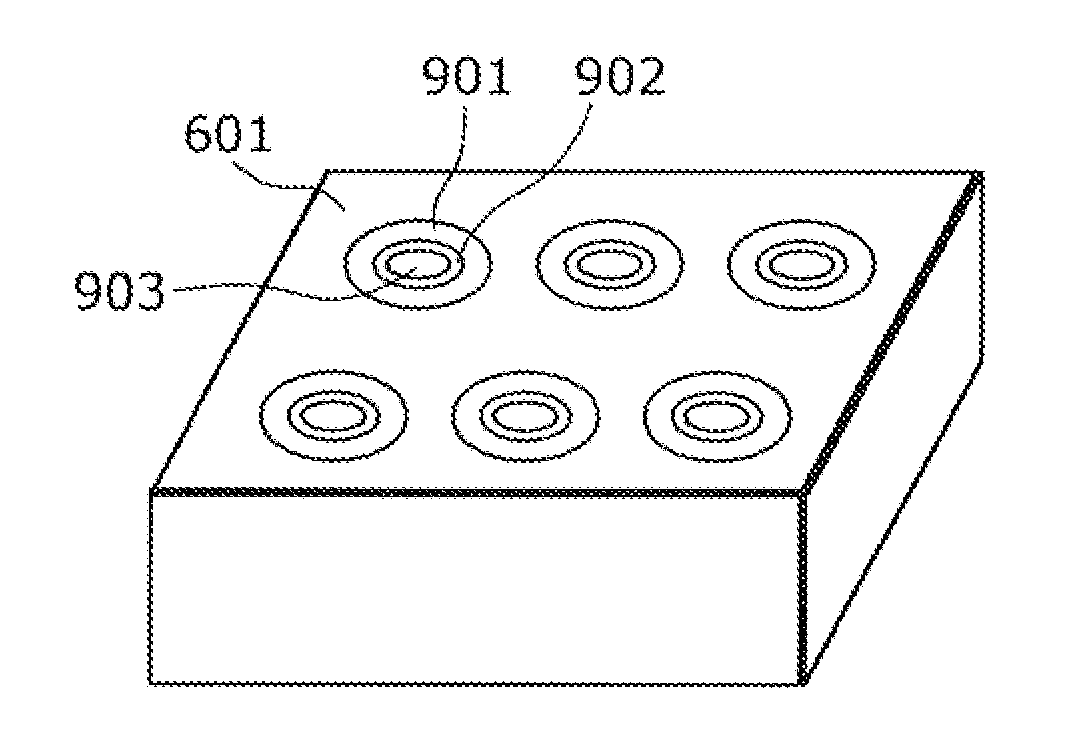
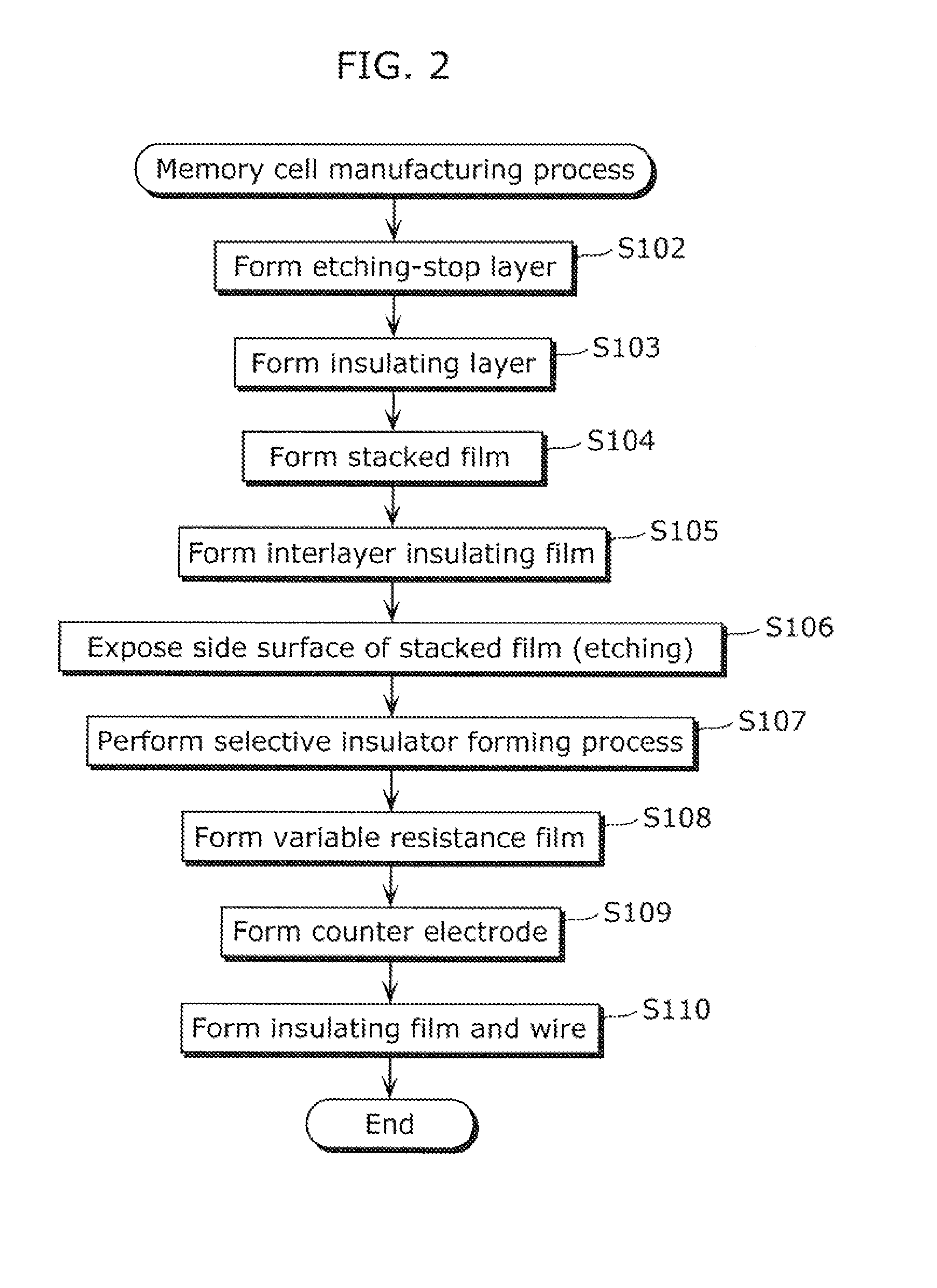
In Embodiment 1, a method of manufacturing a ReRAM in which a variable resistance film is provided in a side surface of an electrode shall be described using FIGS. 1 to 9. It should be noted that these diagrams are intended for showing the positional relationship of respective components and thus thickness and length proportions are not uniform. Furthermore, although plural memory cells are normally formed within the substrate surface, FIGS. 3 to 9 show a cross-sectional view of a vicinity of one cell among these memory cells.

FIG. 1 is an outline configuration diagram of a memory cell of a ReRAM. A semiconductor memory such as the ReRAM requires circuits for driving respective memory cells. These can make use of semiconductor integrated circuits manufactured using the usual CMOS process and so on. Although a memory cell and a drive circuit can be connected by wiring after being manufactured in separate substrates, integrating the memory cell and the drive circuit on the same substra...

embodiment 2

In Embodiment 2, the case of implementing the present invention in the forming of an MRAM shall be described using FIGS. 10 to 14. FIG. 10 is a flowchart for describing a manufacturing process of the memory cell of the MRAM, and FIGS. 11 to 14 are diagrams showing the manufacturing process of the memory cell. These diagrams are intended for showing the positional relationship of respective layers and thus thickness and length proportions are not uniform. Furthermore, although these diagrams show a cross-sectional view of the vicinity of one cell, in actuality, plural cells may be formed within the same substrate.

In the case of the MRAM, the cause for the occurrence of resistance change is not the change in the characteristics of the resistance, and so on, in the insulating film-side as in the ReRAM, but the change in the characteristics of the ferromagnet making up the electrodes formed on both upper and lower surfaces of a tunnel insulating film which is a semiconductor layer. For ...

embodiment 3

In Embodiment 3, the case of an ReRAM having a cell format in which an electrode and a variable resistance film are stacked in a perpendicular direction with respect to the substrate, and plural memories are formed in a planar manner shall be described using FIGS. 15 to 20. FIG. 15 is a flowchart for describing a manufacturing process of a memory cell of the ReRAM, and FIGS. 16 to 20 are diagrams showing the manufacturing process of the memory cell. These diagrams are also intended for showing the positional relationship of respective layers and thus thickness and length proportions are not uniform. Furthermore, although these diagrams show a cross-sectional view of the vicinity of one cell, in actuality, plural cells may be formed within the same substrate.

This cell format also requires drive circuits (semiconductor integrated circuits) for cell driving, and it is preferable that these drive circuits be manufactured on the semiconductor substrate before hand using a CMOS process, a...


PUM


Abstract

The method of manufacturing a semiconductor memory includes a process of forming a projection by performing an insulator forming process on the exposed side surface of a reactive conductive material and a non-reactive conductive material that are stacked above a substrate so as to change a predetermined length of the side surface of the reactive conductive material into an insulator, and thereby causing the side surface of the non-reactive conductive material to project outward from the side surface of the reactive its conductive material. The insulator forming process is an oxidation process or a nitridation process, the reactive conductive material is a material that reacts chemically and changes into the insulator in the oxidation process or nitridation process, and the non-reactive conductive material is a material that does not change into the insulator in the oxidation process or nitridation process.

Description

BACKGROUND OF THE INVENTION(1) Field of the InventionThe present invention relates to a method of manufacturing a semiconductor memory in which information is stored by applying voltage and causing current to flow between electrodes to induce a change of state.(2) Description of the Related ArtCurrently, two types of memories, namely, Dynamic Random Access Memories (DRAMs) and flash memories, are widely used as large-scale integrated storage elements.DRAMs are what are called volatile memories which allow fast writing and reading but require power consumption for memory retention. Therefore, DRAMs are mainly used in short-term memories such as the main memory, and the like, of a computer. Flash memories are what are called nonvolatile memories which do not require power consumption for memory retention. These storage elements have the drawback of low-speed information writing and rewriting, and are thus mainly used in long-term memories for digital cameras and music players.If a sto...

Claims


Application Information

Patent Timeline
Patent Type & Authority Applications(United States)
IPC IPC(8): H01L21/02
CPCH01L27/101H01L27/222H01L43/12H01L45/1273H01L45/146H01L27/249H01L45/04H01L45/1233H01L45/16H10B61/00H10B63/845H10N70/20H10N70/823H10N50/01H10N70/8418H10N70/011H10N70/826H10N70/8833
Inventor NOZAWA, KATSUYA
Owner PANASONIC CORP
Why Eureka
Try Eureka