Gallium nitride crystal substrate and method of producing same

a technology of gallium nitride and crystal substrate, which is applied in the direction of crystal growth process, polycrystalline material growth, chemically reactive gas growth process, etc., to achieve the effect of reducing dislocation, reducing bending (distortion) of gan wafer, and low distortion of gan wafer

Inactive Publication Date: 2007-03-22
SUMITOMO ELECTRIC IND LTD
View PDF4 Cites 17 Cited by
  • Summary
  • Abstract
  • Description
  • Claims
  • Application Information

AI Technical Summary

Benefits of technology

[0014] This invention proposes a low-distortion GaN substrate and a method of producing a low-distortion GaN substrate.
[0015] A GaN substrate 1 of Preferable Version 1 of the present invention includes a matrix crystal regions (R) 11(=low dislocation single crystal regions (Z) and C-plane growth regions (Y): R=Z+Y), voluminous defect accumulating regions (H) 21, c-axis gross core regions (F) 31 and random defect bundle regions (G) 12, which is denoted by FIG. 1(b). The voluminous defect accumulating regions (H) have c-axes inverse to the c-axis of the matrix crystal regions (R) and a-axes similar to the a-axis of the matrix crystal regions (R=Z+Y). The c-axis gross core regions (F) 31, each of which includes at least one crystal, have a-axes different from the a-axis of the matrix crystal regions (R=Z+Y) and a c-axis parallel to the c-axis of the matrix crystal regions (R=Z+Y). 0.1 / cm2 to 10 / cm2 c-axis gross core regions (F) are included in the GaN substrate.
[0016] The GaN substrate of the present invention includes c-axis gross core regions (F), one of which contains more than one crystal having an a-axis different from, and a c-axis common with the low dislocation single crystal regions (Z) and C-plane growth regions (Y). Dislocations newly happen at interfaces between the c-axis gross core regions (F) and low dislocation single crystal regions (Z). New production of dislocations decreases the bending (distortion) of a GaN wafer. Low distortion GaN wafers can be obtained.
[0017]FIG. 7(a) and FIG. 7(b) show the facet growth method proposed by (1) Japanese Patent Laying Open No. 2003-165799 and (2) Japanese Patent Laying Open No. 2003-183100 for decreasing dislocations. The facet growth method reduces dislocations by forming masks 20 with openings on an undersubstrate 10, growing a gallium nitride crystal, forming facets 11f in addition to C-planes 11c, which is a principal plane, converging dislocations into voluminous defect accumulating regions (H) 21 formed at facet pit bottoms on the masks 20 by the function of the facets, combining plus sign dislocations with minus sign dislocations in the voluminous defect accumulating regions (H), and extinguishing dislocations in the low dislocation single crystal regions (Z) and C-plane growth regions (Y).
[0018] In the facet growth method proposed by the Prior Patent Documents (1) and (2), dislocations are reduced by combination of different sign dislocations in the voluminous defect accumulating regions (H) during the growth. A reducing dislocation density gradient occurs in the vertical direction. The progress of growth increases the difference of dislocation density between a near-top plane 11t and a near-bottom plane 11s. A big difference of dislocation density causes strong distortion to the GaN substrate wafer sliced from the facet-growth GaN crystal. FIG. 7(b) is a section of a GaN wafer 1 obtained by slicing the Fig.(a) crystal in planes 11t and 11s. The GaN wafer has large distortion, which is equivalent to a small curvature radius, due to the decreasing dislocation gradient.
[0019] On the contrary, the present invention makes a gallium nitride crystal having c-axis gross core regions (F) 31 and produces new dislocations at interfaces between the c-axis gross core regions (F) 31 and low dislocation single crystal regions (Z) 11. New production of dislocations by the c-axis gross core regions (F) 31 suppresses the vertical reduction of dislocations. The dislocation difference between the near-top plane 11t and the near-bottom plane 11s is decreased by the new generation of dislocations made by the c-axis gross core regions (F) 31. Uniform dislocation density distribution has a function of reducing the distortion of the GaN wafer obtained from the grown GaN crystal by cutting in planes 11t and 11s.

Problems solved by technology

Ununiformity of epitaxial layers prohibits the GaN wafers from making semiconductor devices having uniform properties.

Method used


Image

  • Gallium nitride crystal substrate and method of producing same
  • Gallium nitride crystal substrate and method of producing same
  • Gallium nitride crystal substrate and method of producing same

Examples


embodiment 1

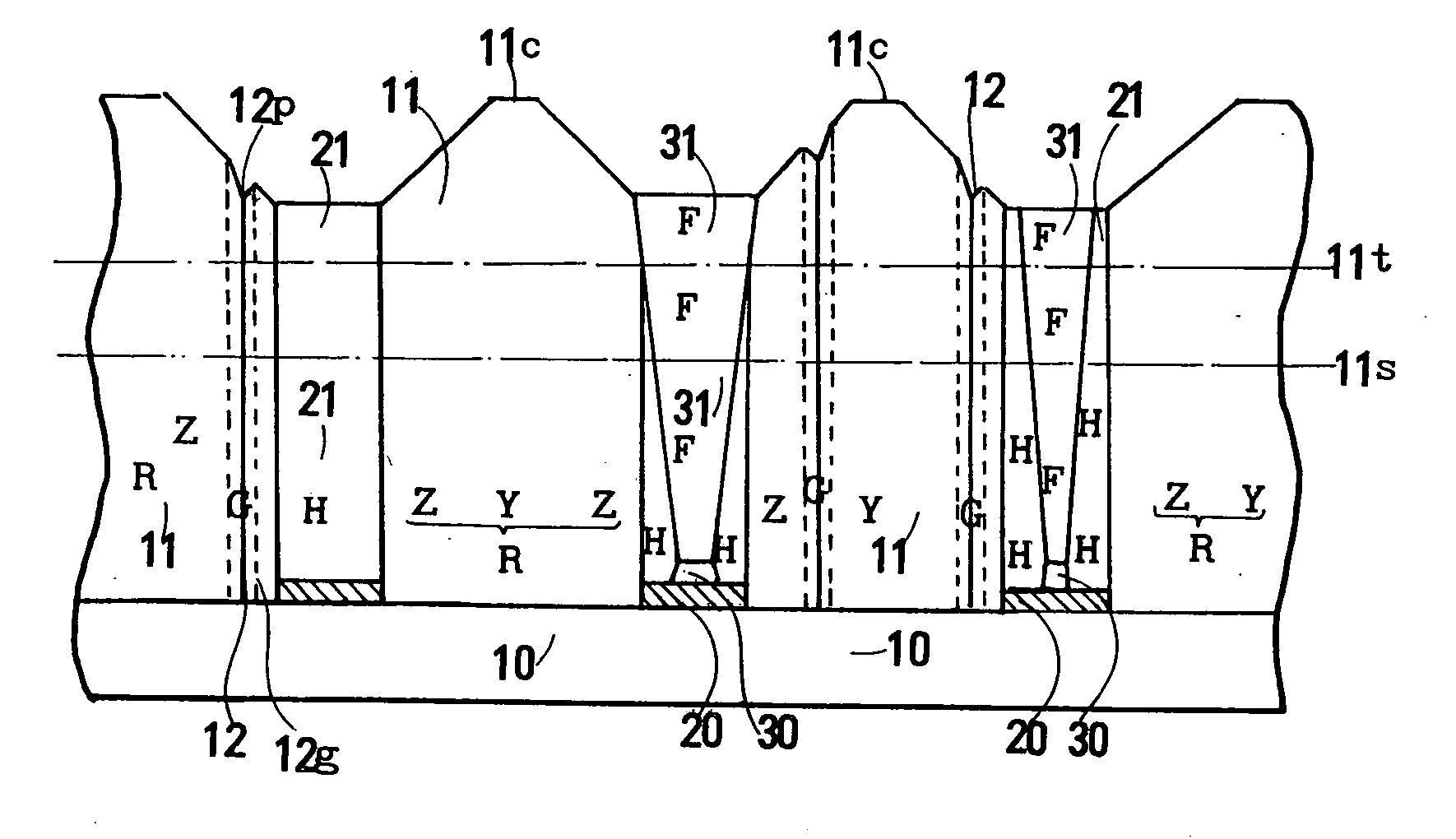
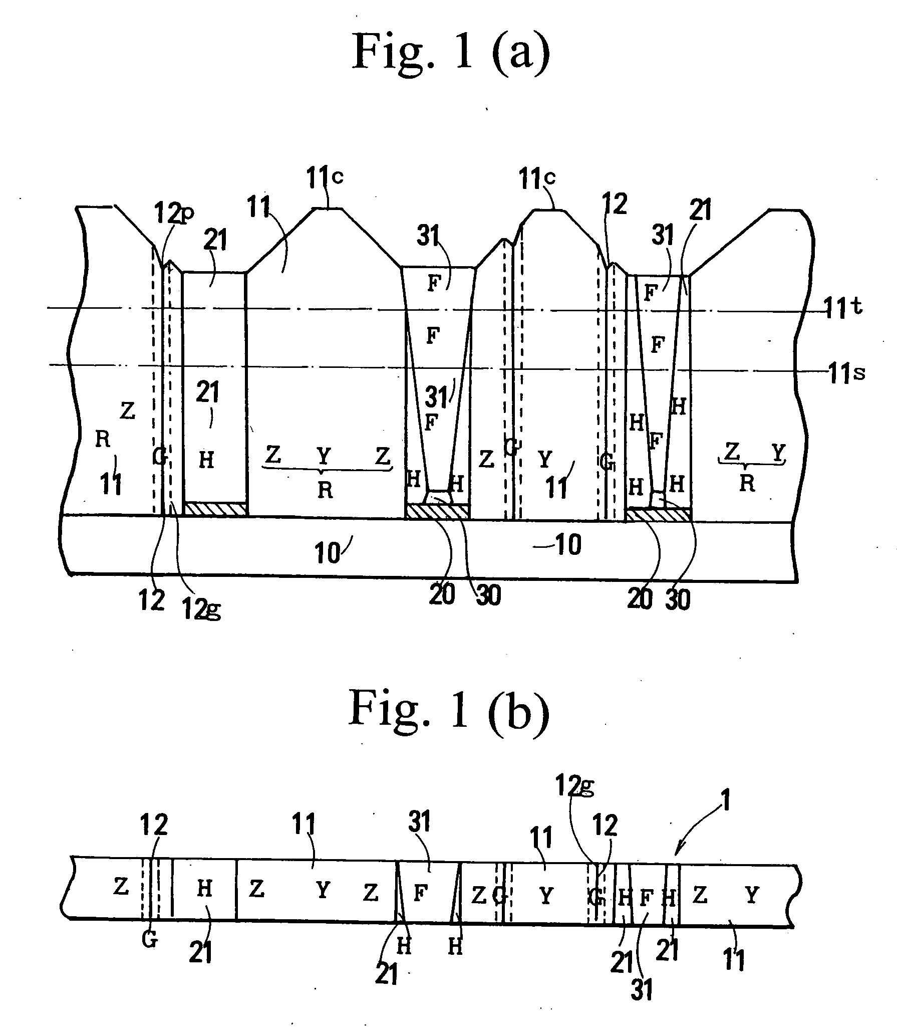
[0055] An undersubstrate is a GaN / sapphire substrate prepared by growing epitaxially a 2 μm thick GaN layer by an MOCVD method on a 5.08 cm wide, 0.4 mm thick sapphire single crystal substrate. Sputtering and etching make a mask Pattern A of a silicon dioxide film (SiO2) on the GaN / sapphire undersubstrate. A GaN crystal is grown on the masked GaN / sapphire undersubstrate by an MOCVD method on a growing condition of a growing temperature of 1030° C., a TMG gas partial pressure of 2.53 Pa, an NH3 gas partial pressure of 5.07 kPa and a growth time of 50 hours.

[0056] The MOCVD growth makes a 0.2 mm thick GaN crystal. A 0.15 mm thick GaN wafer is cut from the grown crystal. The GaN wafer is observed by a fluorescence microscope. Existence of low dislocation single crystal regions (Z), C-plane growth regions (Y), voluminous defect accumulating regions (H), c-axis gross core regions (F) and random defect bundle regions (G) is confirmed by the fluorescence microscope observation. The GaN su...

embodiment 2

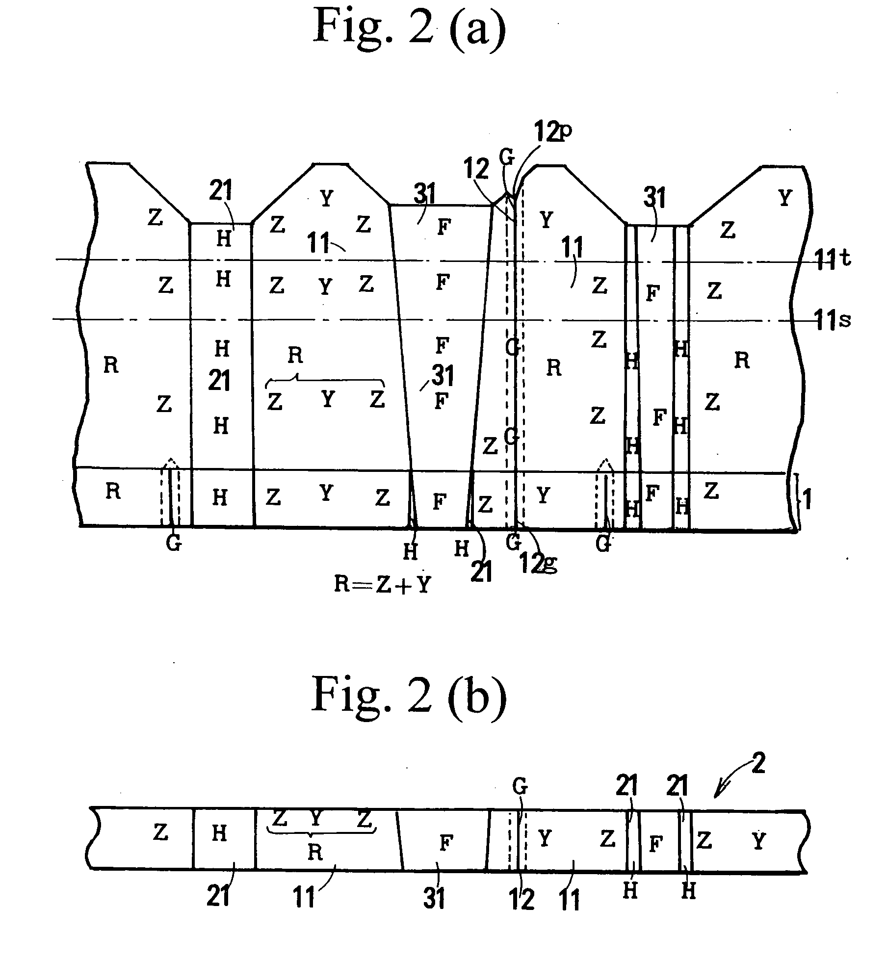
[0058] An undersubstrate is a sapphire single crystal substrate of a 5.08 cm diameter and a 0.4 mm thickness. A mask Pattern B (FIG. 4) of a silicon dioxide (SiO2) film is made on the sapphire undersubstrate by sputtering and etching. A GaN crystal is grown on the masked sapphire undersubstrate by an HVPE method on a growing condition of a growing temperature of 1050° C., a GaCl gas partial pressure of 3.04 kPa, an NH3 gas partial pressure of 35.5 kPa and a growth time of 20 hours.

[0059] The HVPE growth makes a 2.4 mm thick GaN crystal. A 0.45 mm thick GaN wafer is cut from the grown crystal. The GaN wafer is observed by a fluorescence microscope. Existence of low dislocation single crystal regions (Z), C-plane growth regions (Y), voluminous defect accumulating regions (H), c-axis gross core regions (F) and random defect bundle regions (G) is confirmed by the fluorescence microscope observation. The GaN substrate of Embodiment 2 has a 0.5 / cm2 density of the c-axis gross core region...

embodiment 3

[0061] Embodiment 3 GaN crystals are produced by a HVPE method on a condition similar to Embodiment 2 except the mask pattern. Embodiment 3 employs another mask of Pattern C (Stripe mask) as shown in FIG. 5 instead of Pattern B (FIG. 4) of Embodiment 2. The HVPE growth produces a 2.4 mm thick GaN crystal. A 0.45 mm thick GaN substrate is obtained by cutting the as-grown GaN crystal. Embodiment 3 GaN wafer includes low dislocation single crystal regions (Z), C-plane growth regions (Y), voluminous defect accumulating regions (H), c-axis gross core regions (F) and random defect bundle regions (G). The density of c-axis gross core regions (F) with diameters less than 1 mm (d2 in Embodiment 3. The density of random defect bundle regions (G) with diameters less than 500 μm (d2 in Embodiment 3. The curvature radius of the GaN wafer is 530 cm, which corresponds to small distortion. Table 1 denotes the results of Embodiment 3.


PUM

PropertyMeasurementUnit
partial pressureaaaaaaaaaa
anglesaaaaaaaaaa

Abstract

A low-distortion gallium nitride crystal substrate including low dislocation single crystal regions (Z) having a definite c-axis and a definite a-axis, C-plane growth regions (Y) having a c-axis and a-axis parallel to the c-axis and a-axis of the low dislocation single crystal regions (Z), voluminous defect accumulating regions (H) having a c-axis inverse to the c-axis of the low dislocation single crystal regions (Z) and an a-axis parallel with the a-axis of the low dislocation single crystal regions (Z), and 0.1/cm2 to 10/cm2 c-axis gross core regions (F) containing at least one crystal having a c-axis parallel to the c-axis of the low dislocation single crystal regions (Z) and an a-axis different from the a-axis of the low dislocation single crystal regions (Z).

Description

RELATED APPLICATIONS [0001] This application is a continuation-in-part application of U.S. patent application Ser. No. 10 / 933,291 filed on Sep. 3, 2004 and Ser. No. 10 / 936,512 filed on Sep. 9, 2004.BRIEF DESCRIPTION OF THE INVENTION [0002] This invention relates to a low-distortion gallium nitride (GaN) crystal substrate with small distortion and a method of producing a low-distortion gallium nitride substrate. Low-distortion gallium nitride wafers of the present invention can be widely utilized as substrate wafers for making light emitting diodes (LEDs), laser diodes (LDs) and other semiconductor devices. BACKGROUND OF THE INVENTION [0003] Gallium nitride crystal substrates are widely used as substrates of a variety of semiconductor devices. Improvement of properties of semiconductor devices requires low dislocation density GaN wafers. [0004] (1) Japanese Patent Laying Open No. 2003-165799 and (2) Japanese Patent Laying Open No. 2003-183100 newly proposed facet-growth methods for m...

Claims


Application Information

Patent Timeline
Patent Type & Authority Applications(United States)
IPC IPC(8): C30B25/00C30B23/00C30B28/12C30B28/14
CPCC30B25/04C30B29/406C30B29/40C30B25/18
Inventor SATO, FUMITAKANAKAHATA, SEIJI
Owner SUMITOMO ELECTRIC IND LTD
Why Eureka
Try Eureka