Semiconductor device and method for manufacturing semiconductor device

a semiconductor device and semiconductor technology, applied in semiconductor devices, instruments, electrical devices, etc., can solve the problems of increasing the power consumption of the semiconductor device, shortening the traveling distance, and limited uptime, so as to reduce the manufacturing cost

Active Publication Date: 2011-08-11
SEMICON ENERGY LAB CO LTD
View PDF24 Cites 40 Cited by
  • Summary
  • Abstract
  • Description
  • Claims
  • Application Information

AI Technical Summary

Benefits of technology

Further, the transistor which includes the highly purified oxide semiconductor layer whose hydrogen concentration is sufficiently reduced can be formed over...

Problems solved by technology

Especially in portable semiconductor devices, power is supplied from a battery; therefore, uptime is limited due to limited amount of electric power.
For example, in the case of an electric vehicle, leakage current of an in-vehicle semiconductor device shortens the traveling distance per a certain amount of charging.
Such leakage current causes an increase in power consumption of the semiconductor device in a standby period.
For a miniaturized transistor, a gate insulating layer is ...

Method used


Image

  • Semiconductor device and method for manufacturing semiconductor device
  • Semiconductor device and method for manufacturing semiconductor device
  • Semiconductor device and method for manufacturing semiconductor device

Examples


embodiment 1

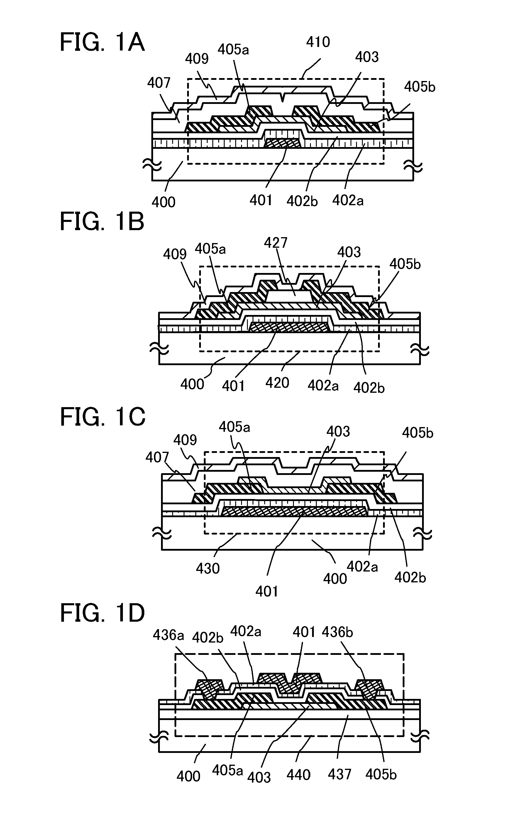
In this embodiment, an example of a transistor that can be applied to a semiconductor device disclosed in this specification will be described. There is no particular limitation on a structure of the transistor that can be applied to the semiconductor device disclosed in this specification. For example, a staggered transistor, a planar transistor, or the like having a top-gate structure in which a gate electrode is provided above an oxide semiconductor layer with a gate insulating layer interposed therebetween or a bottom-gate structure in which a gate electrode is provided below an oxide semiconductor layer with a gate insulating layer interposed therebetween, can be used. The transistor may have a single-gate structure including one channel formation region, a double-gate structure including two channel formation regions, or a triple-gate structure including three channel formation regions. Alternatively, the transistor may have a dual-gate structure having two gate electrodes, on...

embodiment 2

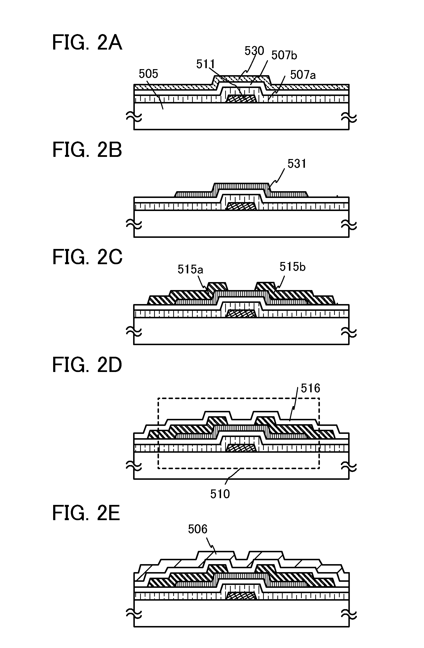
In this embodiment, an example of a transistor including an oxide semiconductor layer and an example of a method for manufacturing the transistor will be described in detail with reference to FIGS. 2A to 2E. The same portion as or a portion having a function similar to those in the above embodiment can be formed in a manner similar to that described in the above embodiment, and also the steps similar to those in the above embodiment can be performed in a manner similar to that described in the above embodiment, and repetitive description is omitted. In addition, detailed description of the same portions is not repeated.

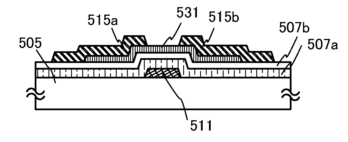
FIGS. 2A to 2E illustrate an example of a cross-sectional structure of a transistor. A transistor 510 illustrated in FIGS. 2A to 2E is a bottom-gate inverted-staggered transistor which is similar to the transistor 410 illustrated in FIG. 1A.

Steps of manufacturing the transistor 510 over a substrate 505 will be described below with reference to FIGS. 2A to 2E.

First, af...

embodiment 3

In this embodiment, an example of forming a dual-gate transistor including two gate electrodes, one of which is provided above a channel region with a gate insulating layer interposed therebetween and the other of which is provided below the channel formation region with another gate insulating layer interposed therebetween will be described below.

Note that since steps in the middle of a manufacturing process are the same as steps in Embodiment 2, description will be made using the same reference numerals for the same portions.

FIGS. 3A to 3C illustrate an example of a cross-sectional structure of a transistor. FIG. 3A is the same as FIG. 2C. First, in accordance with Embodiment 2, a state illustrated in FIG. 3A is obtained.

Next, an insulating layer 516 serving as a protective insulating film is formed in contact with part of the oxide semiconductor layer in a manner similar to that of Embodiment 2. In this embodiment, in order to form a second gate electrode in a later step, an insu...


PUM


Abstract

In a miniaturized transistor, a gate insulating layer is required to reduce its thickness; however, in the case where the gate insulating layer is a single layer of a silicon oxide film, a physical limit on thinning of the gate insulating layer might occur due to an increase in tunneling current, i.e. gate leakage current. With the use of a high-k film whose relative permittivity is higher than or equal to 10 is used for the gate insulating layer, gate leakage current of the miniaturized transistor is reduced. With the use of the high-k film as a first insulating layer whose relative permittivity is higher than that of a second insulating layer in contact with an oxide semiconductor layer, the thickness of the gate insulating layer can be thinner than a thickness of a gate insulating layer considered in terms of a silicon oxide film.

Description

TECHNICAL FIELDThe present invention relates to a transistor including an oxide semiconductor, a semiconductor device including an integrated circuit which includes the transistor, and a method for manufacturing the semiconductor device. For example, the present invention relates to an electronic device on which a semiconductor integrated circuit is mounted as a component.In this specification, a “semiconductor device” refers to any device which can function by utilizing semiconductor characteristics, and a display device, an electro-optical device, a semiconductor circuit, an electronic component, and an electronic device are all included in the category of the semiconductor device.BACKGROUND ARTIn recent years, semiconductor devices have been developed, and a variety of semiconductor devices such as one with a silicon wafer or a glass substrate, which depends on the usage, has been manufactured.For example, in a liquid crystal display device, a transistor and a wiring are formed o...

Claims


Application Information

Patent Timeline
IPC IPC(8): H01L29/12H01L21/36
CPCH01L21/02554H01L21/02565H01L29/7869H01L27/1225H01L29/4908H01L21/02631G02F1/1362H01L29/42384H01L29/495H01L29/513H01L29/517
Inventor ENDO, YUTASAITO, TAKAYUKIYAMAZAKI, SHUNPEI
Owner SEMICON ENERGY LAB CO LTD
Why Eureka
Try Eureka