method and apparatus to prepare a substrate for molecular detection

a substrate and molecular detection technology, applied in the field of methods and apparatus to prepare a substrate for molecular detection, can solve the problems of uneven active area of sers, smooth thin films, and conventional thin film growth techniques, and achieve enhanced coherent anti-stokes raman spectroscopy, enhanced infrared absorption, and the effect of improving the detection efficiency

Inactive Publication Date: 2011-08-11
IMRA AMERICA
View PDF21 Cites 30 Cited by
  • Summary
  • Abstract
  • Description
  • Claims
  • Application Information

AI Technical Summary

Benefits of technology

[0011]The present invention comprises a method of forming a SERS active metal surface on a substrate for Raman spectroscopy and the product formed by the method. The method comprises the steps of providing a substrate or support material having a relatively flat surface and applying a nano-structured metal layer to the surface in a single step by a process comprising ultrashort pulsed laser deposition, ultrashort backside transfer pulsed laser deposition, or sputtering, thereby forming the substrate for Raman spectroscopy. The product can be used in surface enhanced Raman spectroscopy (SERS), surface enhanced resonance Raman spectroscopy (SERRS), surface enhanced hyper Raman spectroscopy (SEHRS), surface enhanced coherent anti-Stokes Raman spectroscopy (SECARS), and surface enhanced infrared absorption (SEIRA). The method is rapid, inexpensive, highly reproducible and tunable for optimization of detection based on the active metal used or the substance being detected. The method permits a thickness gradient of the active metal layer to be applied to the surface so that the optimum thickness for detection of a compound of interest can easily be determined by coordinating signal intensity with position on the gradient. The method also permits the substrate surface to be pre-coated with other materials prior to applying the active metal surface to enhance the Raman signal derived from the active metal layer. In this embodiment, the SERS active metal is not directly bonded to the substrate surface.

Problems solved by technology

The chemical theory, however, only applies to species that have formed a bond with the surface so it can not explain the enhancement in all cases whereas the electromagnetic theory is broader in application.
Because SERS requires a rough metal surface, conventional thin film growth techniques, which produce smooth thin films, are not suitable for forming SERS substrates.
One method for making a SERS substrate is to drop-cast or spread, a solvent, which contains nanoparticles, onto a surface; however, this method suffers from non-uniformity of the SERS active area, a lack of reproducibility, and inconsistent signal enhancement.
This method is relatively simple and may be used on large-scale applications; however, the stability of the nanoparticle solution can be an issue.
This method requires several steps to obtain the desired SERS substrate and is typically expensive due to the required equipment used to produce the surfaces such as photo- or electron- lithography.
This method claims to be inexpensive compared with other patterned substrates based on lithography techniques discussed above, but it is still a multistep process and time consuming.

Method used


Image

  •  method and apparatus to prepare a substrate for molecular detection
  •  method and apparatus to prepare a substrate for molecular detection
  •  method and apparatus to prepare a substrate for molecular detection

Examples


Embodiment Construction

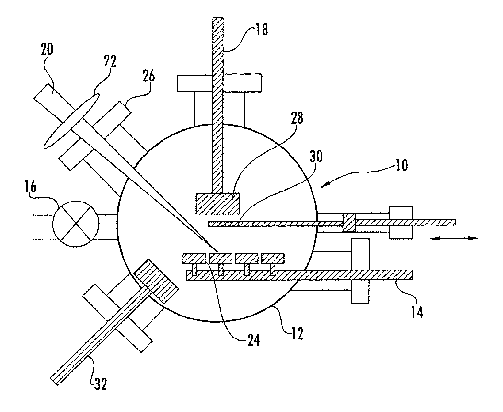
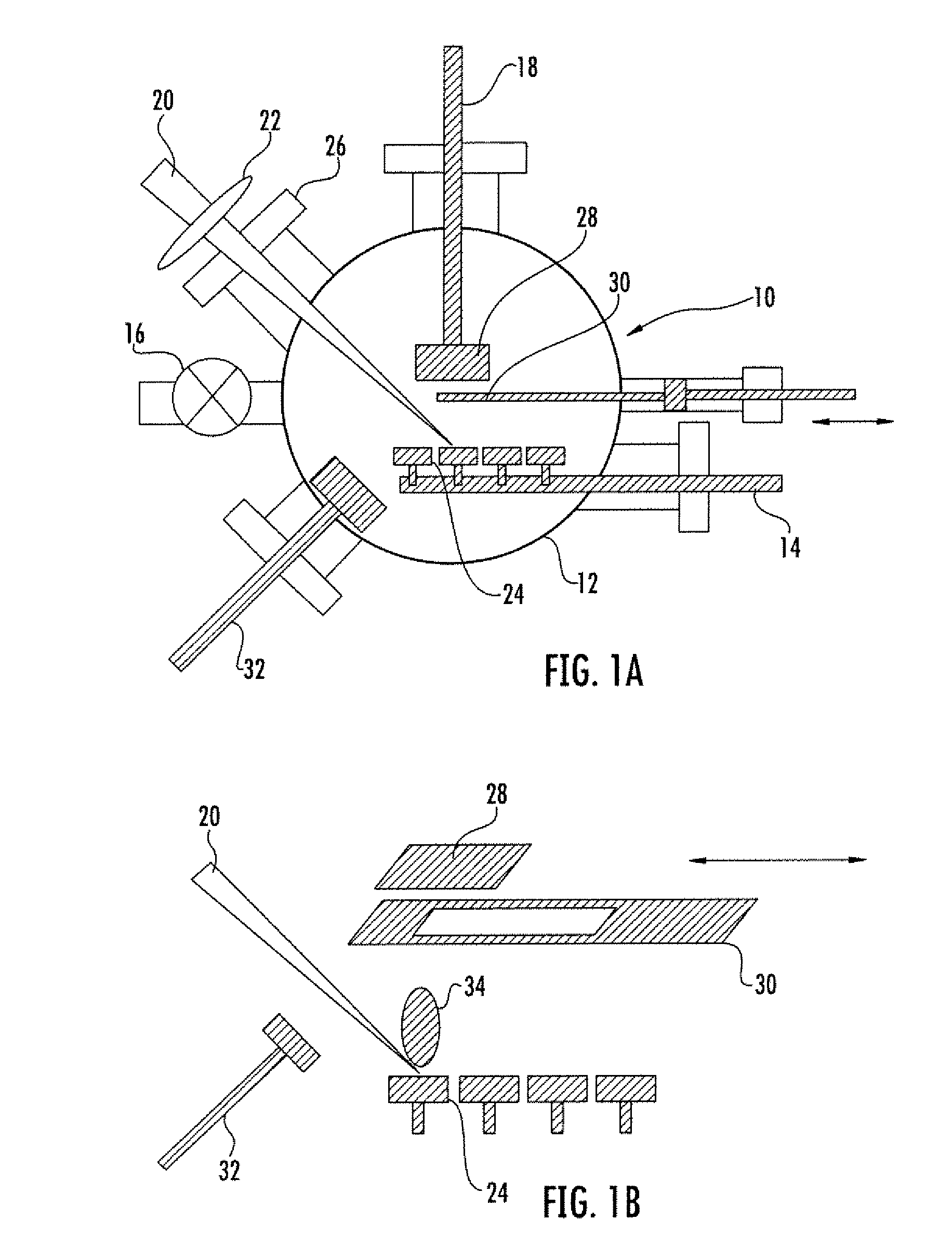
[0025]As noted above, it is highly desirable to develop a method for producing a SERS active metal surface on a substrate that is inexpensive, rapid to carry out, highly reproducible, and tunable for detection of various substances including organic and biological molecules. The present invention is a simplified one step process for preparing SERS actaive metal surfaces on substrates having improved reliability, improved reproducibility, reduced cost, and being tunable for optimization of the detection of specific molecules. The present invention utilizes pulsed laser deposition (PLD), particularly using ultrafast lasers, to fabricate a functional SERS active metal surface on a surface of a support material in a single step process. When compared to the commercially available SERS substrate, Klarite®, a SERS substrate prepared according to the present invention shows a better sample detection signal with less fluorescent background signal from the substrate. As noted above, the SERS...


PUM

PropertyMeasurementUnit
sizeaaaaaaaaaa
sizeaaaaaaaaaa
thicknessaaaaaaaaaa

Abstract

An device for Raman spectroscopy such as surface enhanced Raman spectroscopy (SERS) is disclosed herein. Various embodiments may be utilized to prepare a SERS substrate using several deposition techniques such as pulsed laser deposition. Some embodiments optimize coverage, volume, or elements of SERS active metals. The method is a single step inexpensive method for preparing a SERS active substrate. In some embodiments a coating layer underneath the SERS active metals is utilized for additional enhancements.

Description

RELATED APPLICATIONS[0001]This application claims the benefit of U.S. provisional application Ser. No. 61 / 303,014 filed Feb. 10, 2010.[0002]The subject matter of this application is related to U.S. patent application Ser. No. 11 / 405,020 filed on Apr. 17, 2006 and issued on Oct. 27, 2009 as U.S. Pat. No. 7,608,308, entitled “P-type Semiconductor Zinc Oxide Films Process for Preparation Thereof, and Pulsed Laser Deposition Method Using Transparent Substrates”. The subject matter of this application is also related to U.S. patent application Ser. No. 12 / 401,967 entitled “A Method for Fabricating Thin Films”, filed on Mar. 11, 2009, which claims priority to U.S. patent application Ser. No. 12 / 254,076 entitled “A Method for Fabricating Thin Films”, filed on Oct. 20, 2008, and which claims priority to U.S. Provisional Application No. 61 / 039,883, entitled “A Method for Fabricating Thin Films”, filed Mar. 27, 2008. The subject matter of this application is also related to U.S. patent applic...

Claims


Application Information

Patent Timeline
Patent Type & Authority Applications(United States)
IPC IPC(8): G01J3/44C23C14/28C23C14/34G01N21/65B82Y30/00B82Y99/00
CPCB82Y30/00B82Y40/00G01N21/658C23C14/3435C23C14/083
Inventor MURAKAMI, MAKOTOCHE, YONGLIU, BINGICHIKAWA, YUKI
Owner IMRA AMERICA
Why Eureka
Try Eureka