Photovoltaic device and manufacturing method for a photovoltaic device

a photovoltaic cell and manufacturing method technology, applied in the direction of solid-state devices, pv power plants, semiconductor devices, etc., can solve the problem of lowering the characteristics of the photovoltaic cell units themselves, and achieve the effect of suppressing the reduction of characteristics

Inactive Publication Date: 2011-08-18
SANYO ELECTRIC CO LTD
View PDF2 Cites 2 Cited by
  • Summary
  • Abstract
  • Description
  • Claims
  • Application Information

AI Technical Summary

Benefits of technology

[0013]According to the present invention it is possible to suppress reduction in characteristics due to contact between an intermediate layer and a rear surface electrode, in a photovoltaic device, without degrading characteristics of a photovoltaic cell unit.

Problems solved by technology

However, when carrying out laser processing in an oxidizing atmosphere the photovoltaic cell units, which are electricity generating layers, are exposed to oxygen, and a new problem arises in that the characteristics of the photovoltaic cell units themselves are lowered.

Method used


Image

  • Photovoltaic device and manufacturing method for a photovoltaic device
  • Photovoltaic device and manufacturing method for a photovoltaic device
  • Photovoltaic device and manufacturing method for a photovoltaic device

Examples


example

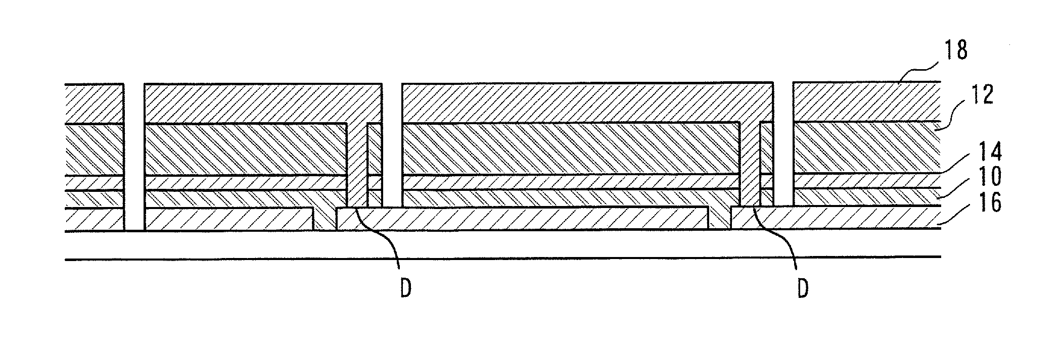
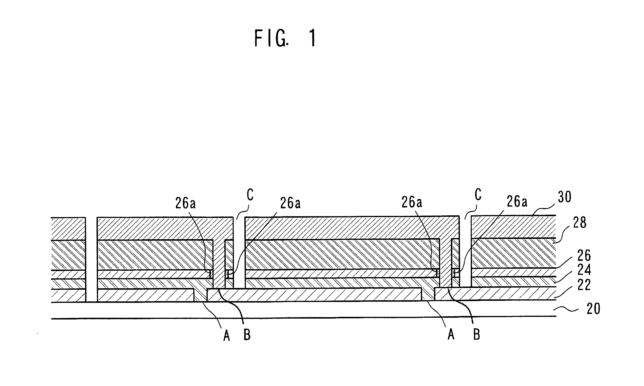
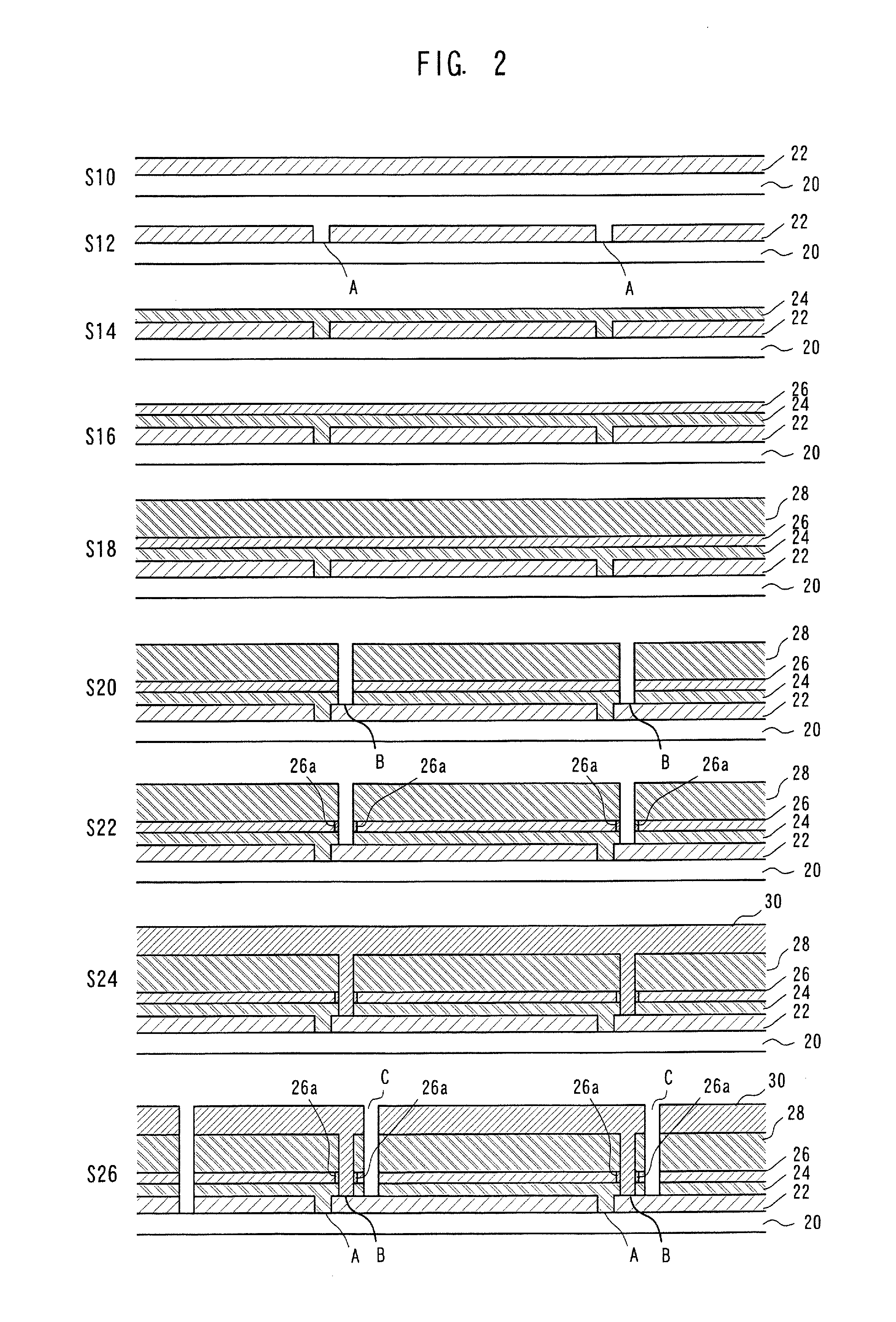
[0033]A surface electrode 22 being an SnO2 film having a textured structure was formed on a glass substrate 20, and an isolation trench A of 40 μm line thickness was formed. After that an amorphous silicon first photovoltaic cell unit 24 having an i-layer film thickness of 250 nm was formed.

[0034]After forming the first photovoltaic cell unit 24, a ZnO film having a film thickness of 50 nm and including aluminum as a dopant was formed as the intermediate layer 26. A microcrystalline silicon second photovoltaic cell unit 28 with an i-layer film thickness of 2000 nm was then formed.

[0035]After formation of the second photovoltaic cell unit 28, an isolation trench B of line width 50 μm was formed using the second harmonic of a Nd:YAG laser of wavelength 532 nm. After that, RF plasma processing is carried out in a nitrogen (N2) or ammonia (NH3) gas atmosphere, causing a higher nitrogen content in the end section 26a of the intermediate layer 26 than in other regions. After nitriding tre...


PUM


Abstract

A photovoltaic device has a first photovoltaic cell unit and a second photovoltaic cell unit stacked on either side of a conductive intermediate layer, between a first electrode and a second electrode, the first electrode and second electrode being electrically connected by a channel formed through the first photovoltaic cell unit, the second photovoltaic cell unit, and the intermediate layer as far as the surface of the first electrode, and a PN junction being formed at an end section of the intermediate layer that contacts the second electrode by adding dopant.

Description

BACKGROUND OF THE INVENTION[0001]1. Field of the Invention[0002]The present invention relates to a photovoltaic device and a manufacturing method for a photovoltaic device.[0003]2. Description of the Related Art[0004]As shown in FIG. 3, a tandem type photovoltaic device having upper and a lower photovoltaic cell units 10, 12 stacked on either side of an intermediate layer 14 is known. One or more types of transparent conductive film are used in the intermediate layer 14 interposed between the upper and lower photovoltaic cell units. Also, a rear surface electrode 18 of silver (Ag) for also serving as a rear surface reflective layer is formed on part of the rear surface electrode, and the rear surface electrode 18 is connected to a front surface electrode 16 by means of a channel D formed penetrating through as far as the front surface electrode 16.[0005]With this type of structure, the intermediate layer 14 interposed between the upper and lower photovoltaic cell units 10, 12 is in ...

Claims


Application Information

Patent Timeline
Patent Type & Authority Applications(United States)
IPC IPC(8): H01L31/0224H01L31/18
CPCH01L31/076Y02E10/548H01L31/043H01L31/046H01L2924/0002H01L2924/00H01L31/0463
Inventor KUNII, TOSHIEYATA, SHIGEO
Owner SANYO ELECTRIC CO LTD
Why Eureka
Try Eureka