Current sink system based on sample and hold for source side sensing
a current sink and source side sensing technology, applied in the field of sensing data in memory devices, can solve the problems of increasing the complexity the noise of the sense amplifier, and the time needed for sensing, so as to reduce the amount of voltage variations, reduce the variation of read current, and tighten the distribution of voltage or current on the sensing node among memory cells in the array.
- Summary
- Abstract
- Description
- Claims
- Application Information
AI Technical Summary
Benefits of technology
Problems solved by technology
Method used
Image
Examples
first embodiment
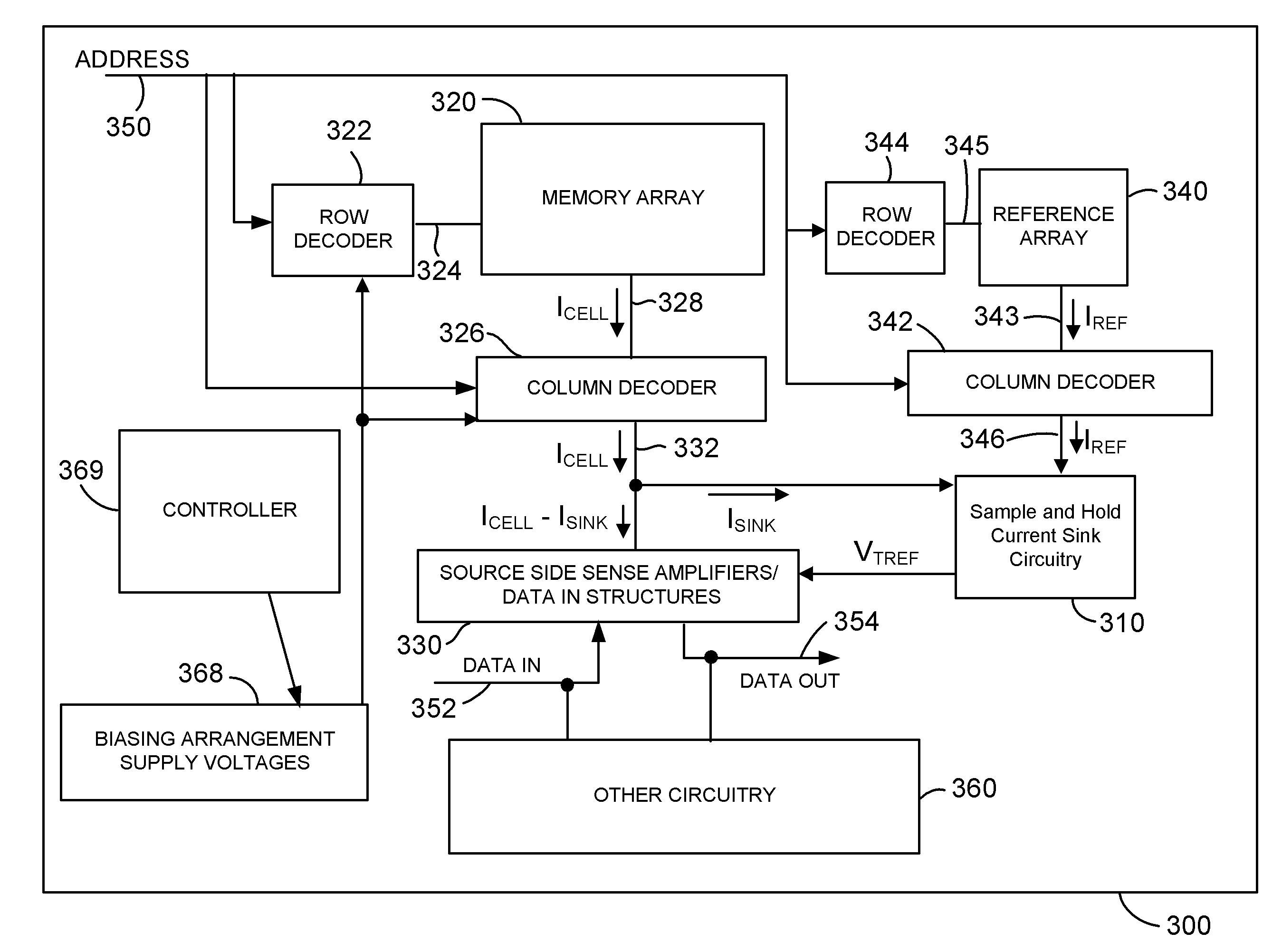
[0055]FIG. 5 is a schematic diagram of the sample and hold current sink circuitry 310 used for sensing a data value stored in a selected memory cell 510 in the memory array 320.
[0056]Word line 324a is coupled to the gate terminal of the memory cell 510. Bit lines 328a, 328b are coupled to the drain and source terminals 511, 512 of the memory cell 510.
[0057]In a sense operation of the memory cell 510, appropriate voltages are applied to word line 324a and bit line 328a to induce a read current ICELL from the drain 511 to the source 512 and onto the bit line 328b. The read current ICELL is provided to the data line 332a via column decoder 326.
[0058]In the illustrated example, reference cell 560 of the reference array 340 is used to provide the reference current IREF. Word line 345a is coupled to the gate terminal of the reference cell 560. Bit lines343a and 343b are coupled to the drain terminal 561 and source terminal 562 of the reference cell 560.
[0059]Voltages are applied to the wo...
second embodiment
[0098]FIG. 7 is a schematic diagram of the sample and hold current sink circuitry 310. In FIG. 7, the load transistor 530 is implemented as a PMOS transistor. The positive input 546 of the operational amplifier 540 is coupled to ground, and the negative input 544 is coupled to the reference line 346a so that a negative feedback path can be established between the output 542 and the negative input 544.
third embodiment
[0099]FIG. 8 is a schematic diagram of the sample and hold current sink circuitry 310. In FIG. 8, the gate terminal of the transistor 522 is selectively coupled to ground by switch 526. Using the switch 526 coupled to ground rather than the input 546 of the operational amplifier 540 can improve the closed loop response time by reducing the capacitance coupled to the reference line 346a.
PUM
 Abstract
Description
Claims
Application Information


