

3D integrated circuit structure, semiconductor device and method of manufacturing same
a technology of integrated circuit and manufacturing method, which is applied in the direction of semiconductor devices, semiconductor/solid-state device details, electrical apparatus, etc., can solve the problems of failure of formed mosfet, new device structures, etc., to achieve the effect of enhancing the performance of 3d integrated circui
- Summary
- Abstract
- Description
- Claims
- Application Information
AI Technical Summary
Benefits of technology
Problems solved by technology
Method used
Image

Examples
first embodiment
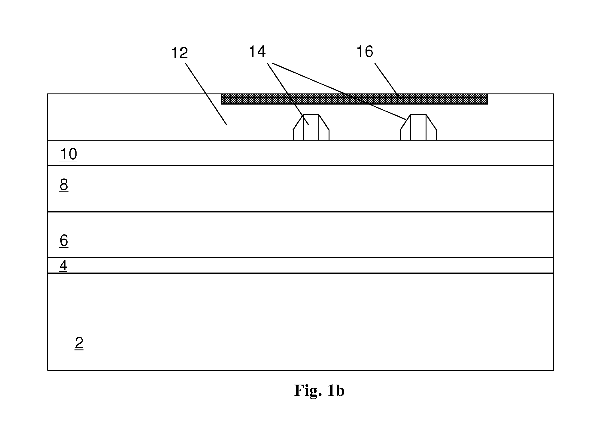
FIGS. 2 and 3 illustrate partial structures of a 3D integrated circuit of a first embodiment formed by using the wafer device 100 of the embodiment of FIG. 1.
In FIG. 2, a diagram of the connection of the formed wafer device 100 for the 3D integrated circuit to an external circuit 300 is shown. Here, the external circuit 300 may be an external power source or external signal I / O. As shown in FIG. 2, a conductive material 22 exposed from the wafer device 100 is connected to the external circuit 300, thereby supplying power to the 3D integrated circuit or performing external signal transmission.
In FIG. 3, besides the connection of the wafer device 100 for the 3D integrated circuit to the external circuit 300, a diagram of the connection for the wafer device 100 to another wafer device 200 of the 3D integrated circuit is also provided. As shown in FIG. 3, the wafer device 200 is turned over, with a via 42 being provided thereon, the via 42 being connected to a BEOL 43 of a MOSFET transi...
second embodiment
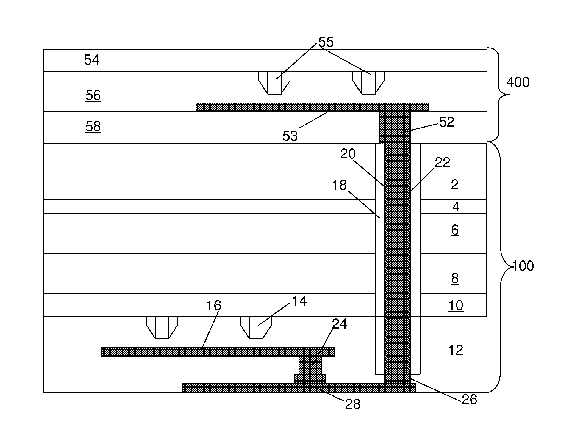
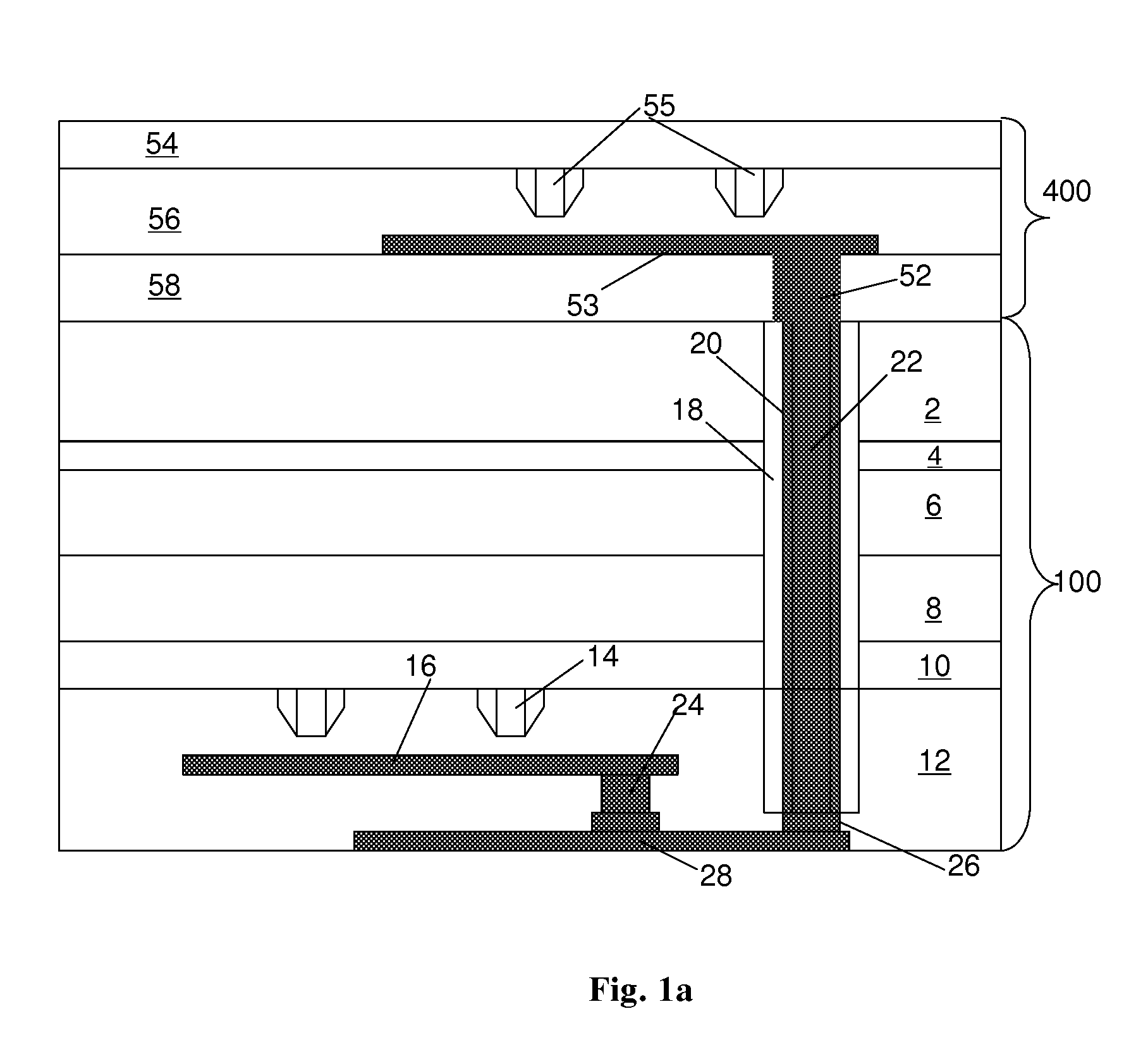
FIG. 4 is a diagram of a partial structure of a 3D integrated circuit of a second embodiment formed by using the wafer device 100 of the embodiment of FIG. 1.
In FIG. 4, the connection of the wafer device 100 for the 3D integrated circuit to another wafer device 400 is provided. As shown in FIG. 4, the wafer device 400 is turned over, with a via 52 being provided thereon, the via 52 being connected to a BEOL 53 of a MOSFET transistor 55 constructed on the wafer device 400. The MOSFET transistor 55, the BEOL 53, and the via 52 of the wafer device 400 are constructed in the same manner as those of the wafer device 100, i.e., the MOSFET transistor 55 is disposed in an oxide layer 56 above the SOI layer 54, and the via 52 is disposed in the oxide layer 58 above the oxide layer 56.
Thus, the wafer 100 is connected to the via 52 through the metal conductive material exposed from its TSV, such that the TSV of the wafer device 100 is connected to the wafer device 200, i.e., connecting the waf...
PUM
 Abstract
Description
Claims
Application Information