Microstructural body and production method therefor

a micro-structural body and production method technology, applied in the direction of variable capacitors, printed circuit non-printed electric components association, instruments, etc., can solve the problems of unstable displacement of the movable portion, unfavorable torsional displacement, etc., to reduce the change and unevenness of function, suppress the transmission of stress, and reduce the effect of change and unevenness

Inactive Publication Date: 2011-09-22
CANON KK
View PDF5 Cites 13 Cited by
  • Summary
  • Abstract
  • Description
  • Claims
  • Application Information

AI Technical Summary

Benefits of technology

[0007]According to the microstructural body of the present invention, since the fixed support portion is fixed to the substrate at one center position, it is possible to suppress transmission of stress to the elastic support portion, which elastically connects the frame-shaped movable portion and the support portion, resulting from the difference in elongation between the substrate and the microstructural body. For example, such difference in elongation is caused by the difference in linear expansion coefficient between the substrate and the microstructural body, the temperature difference during use, and deformation of the substrate. If the stress is applied to the elastic support portion

Problems solved by technology

This makes displacement motion of the movable portion unstable.
Consequentl

Method used


Image

  • Microstructural body and production method therefor
  • Microstructural body and production method therefor
  • Microstructural body and production method therefor

Examples


first example

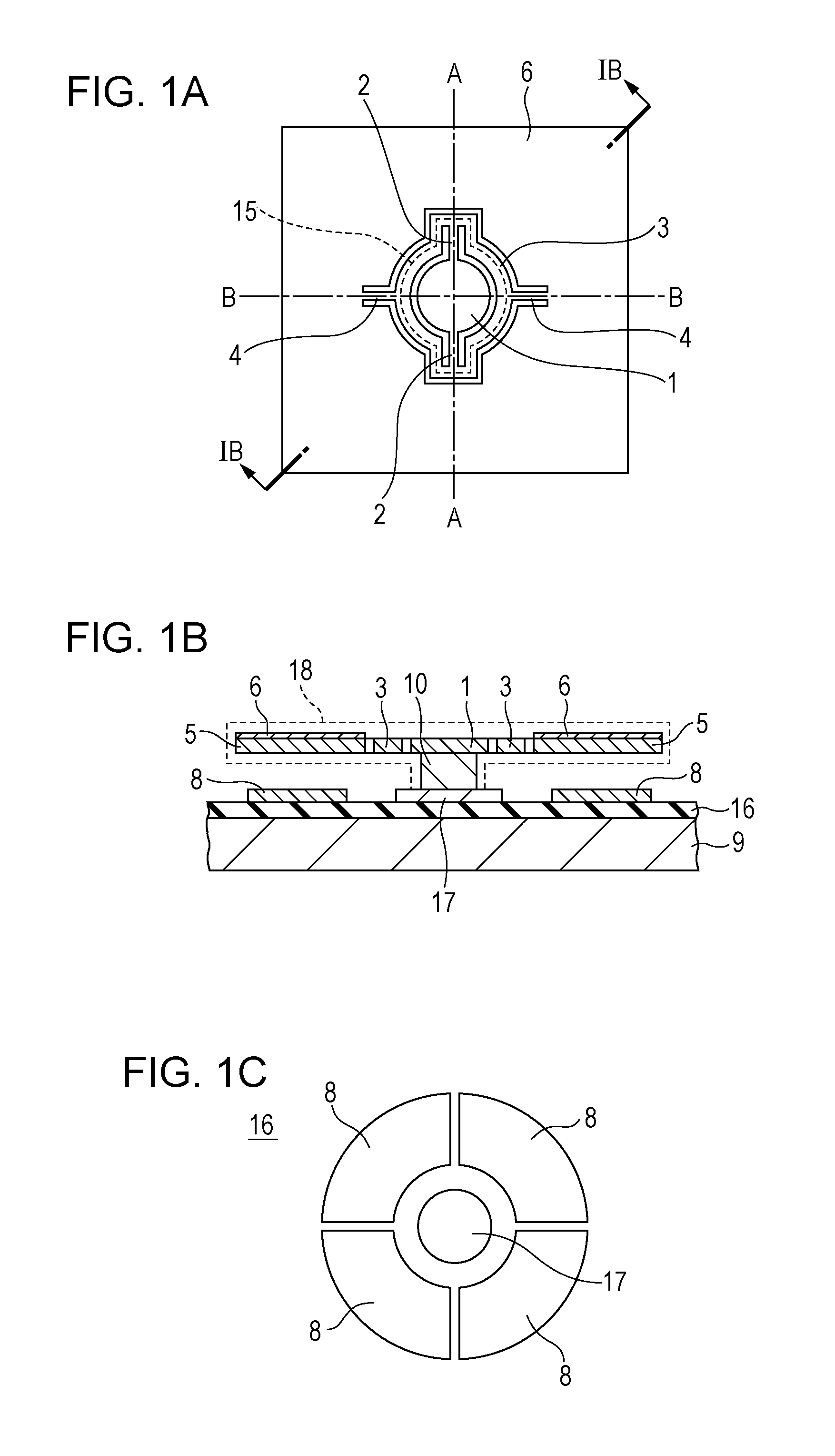
[0038]A microstructural body array 22 according to a first example of the present invention will be described with reference to FIGS. 5A to 5C. FIG. 5A is a top view of each microstructural body 18 of the first example, FIG. 5B is a top view of the microstructural body array 22, and FIG. 5C is a cross-sectional view of the microstructural body array 22. Portions having the same functions as those adopted in the above-described embodiment are denoted by the same reference numerals, and detailed descriptions thereof are omitted.

[0039]In the first example, two pairs of torsion springs 2 and 4 that constitute a center-fixed gimbal structure each have a meandering structure, as illustrated in FIG. 5A. Each microstructural body 18 has the same cross-sectional structure as in FIG. 1B. As illustrated in FIGS. 5B and 5C, a plurality of microstructural bodies 18 of FIG. 5A are arranged on an electrode substrate 9 to form a microstructural body array 22. As in the above-described embodiment, t...

second example

[0041]A microstructural body according to a second example of the present invention will be described with reference to FIGS. 6A and 6B. FIG. 6A is a top view of a MEMS device of the second example, and FIG. 6B is a top view of an electrode substrate 9. Portions having the same functions as those adopted in the embodiment and the first example described above are denoted by the same reference numerals, and detailed descriptions thereof are omitted. In the second example, the electrode substrate 9 is provided with one microstructural body 18. On the electrode substrate 9, fixed electrodes 8 and a receiving portion 17 are provided with leads 13 and electrode pads 14, as illustrated. By electrically connecting the electrode pads 14 to a driving circuit, two-dimensional torsional displacement can be caused in the microstructural body 18.

[0042]The length of one side of the microstructural body 18 is 250 μm, and the diameter of a post 10 is 30 μm. A gap of 10 μm is provided between a mova...

third example

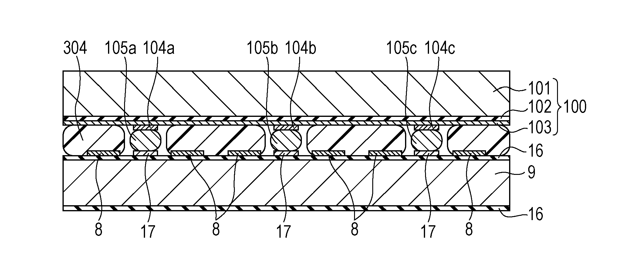
[0044]A production method for a microstructural body array (for example, used as a micromirror array) according to a third example of the present invention will be described with reference to FIGS. 7A to 7C. FIGS. 7A to 7C are cross-sectional views of microstructural bodies taken along line IB-IB of FIG. 1A, and a procedure for producing a microstructural body array including three microstructural bodies will be described here. Referring to FIG. 7A, an SOI substrate (device substrate) 100 including a device layer 103 in which a center-fixed gimbal structure is to be formed later has an SOI (silicon on insulator) structure of single-crystal silicon.

[0045]A description will be given of a step of forming bumps 105a to 105C (hereinafter collectively referred to as bumps 105) on the device layer 103 by Au plating. First, seed portions 104a to 104c (collectively referred to as seed portions 104) are formed. Here, each seed portion 104 is formed by two layers of Au and Cr. The Cr layer is ...


PUM

PropertyMeasurementUnit
Temperatureaaaaaaaaaa
Electric potential / voltageaaaaaaaaaa

Abstract

A microstructural body includes a substrate such as an electrode substrate, a support portion, one post that fixes the support portion to the substrate, a frame-shaped movable portion provided around outer periphery of the support portion, and an elastic support portion that elastically connects the movable portion and the support portion. The elastic support portion supports the frame-shaped movable portion such that the movable portion is movable relative to the support portion. The elastic support portion includes torsion springs and an elastically deformable connecting portion.

Description

BACKGROUND OF THE INVENTION[0001]1. Field of the Invention[0002]The present invention relates to a microstructural body made from a wafer by a semiconductor process, such as micro electro mechanical systems (MEMS), a microstructural body array formed by a plurality of microstructural bodies, and a production method therefor. Here, the term “microstructural body” mainly refers to a structural body that has a minute size of the order of micrometers and that includes a movable portion. For example, the microstructural body can be used in a dynamic quantity sensor (e.g., an acceleration sensor, a pressure sensor, or a gyro sensor), a light deflector, an optical switch, and an optical modulation element.[0003]2. Description of the Related Art[0004]U.S. Patent Application Publication Nos. 2008 / 100898 A1 and 2009 / 067033 A1 disclose micro electro mechanical systems (MEMS) used as an actuator and a sensor. For example, a movable portion is provided on a substrate so that the movable portion ...

Claims


Application Information

Patent Timeline
IPC IPC(8): H01G5/011B23P11/00
CPCB81B7/0048B81B2201/042Y10T29/49837B81C2203/0118G02B26/0841B81B2201/045
Inventor KATO, TAKAHISAWATANABE, SHINICHIRO
Owner CANON KK
Why Eureka
Try Eureka