Optoelectronic Devices

a technology of optoelectronic devices and optical components, applied in the direction of instruments, semiconductor lasers, optical elements, etc., can solve the problems of limited device architecture, additional optical losses that arc, and no device architecture has been proven to be suitable for the realization of electrically pumped organic semiconductor lasers, etc., to achieve low optical losses, low optical losses, and high lfet current

Active Publication Date: 2011-09-22
CAMBRIDGE ENTERPRISE LTD
View PDF19 Cites 18 Cited by
  • Summary
  • Abstract
  • Description
  • Claims
  • Application Information

AI Technical Summary

Benefits of technology

[0031]In embodiments the thickness and dimensions of the individual layers of the LFET and of the waveguide are chosen to achieve incoupling of the light emitted from the LFET into the waveguide, and preferably optimized also to simultaneously achieve (i) low optical losses, and (ii) high LFET current.
[0032]In various embodiments of the present invention, a fabrication method for the LFET described above is provide, with an organic semiconductor active layer and a waveguide integrated within the channel of the light-emitting field-effect transistor, in which thickness and dimensions of the individual layers of the LFET and of the waveguide are chosen to achieve incoupling of the light emitted from the LFET into the waveguide, and preferably also optimized to simultaneously achieve (i) low optical losses, and (ii) high LFET current.
[0033]Various embodiments of the present invention provide a semiconductor laser comprising a light-emitting field effect transistor (LFET), the LFET having a channel which, in operation, conducts charge carriers of two types of opposite polarity, a waveguide optically coupled to said channel of said LFET, and a light reflector configured to provide an optical cavity for said laser.

Problems solved by technology

The reasons for this are related to additional optical losses that arc present when electrical pumping is used, due to presence of electrodes (losses due to absorption of light in electrodes), charge-carrier induced absorptions as well as presence of triplet states.
At present no device architecture has been proven to be suitable realization of an electrically pumped organic semiconductor laser.
However, the aforementioned are limited and there exists a need in the art for additional improvements.

Method used


Image

  • Optoelectronic Devices
  • Optoelectronic Devices
  • Optoelectronic Devices

Examples


Embodiment Construction

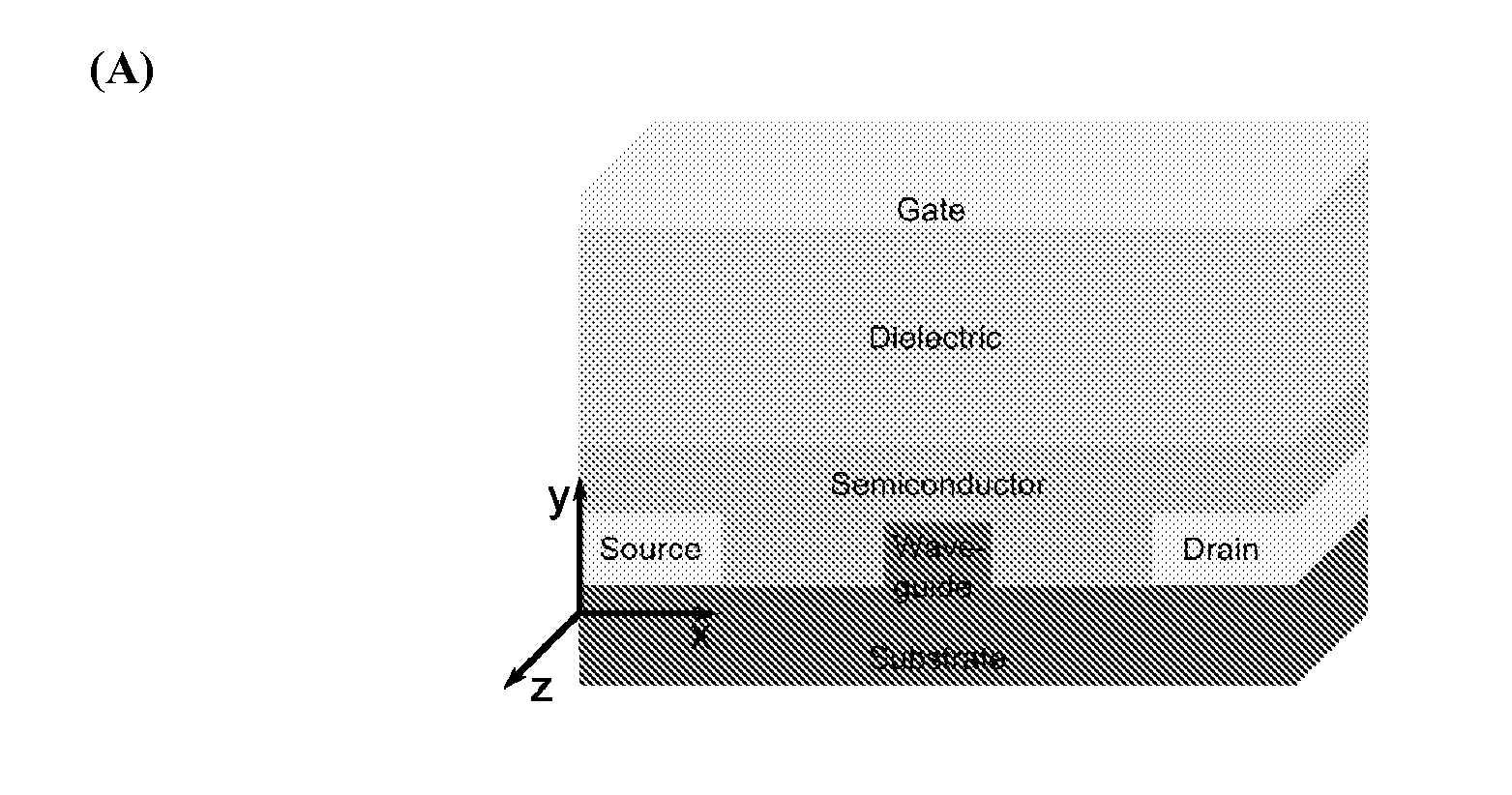
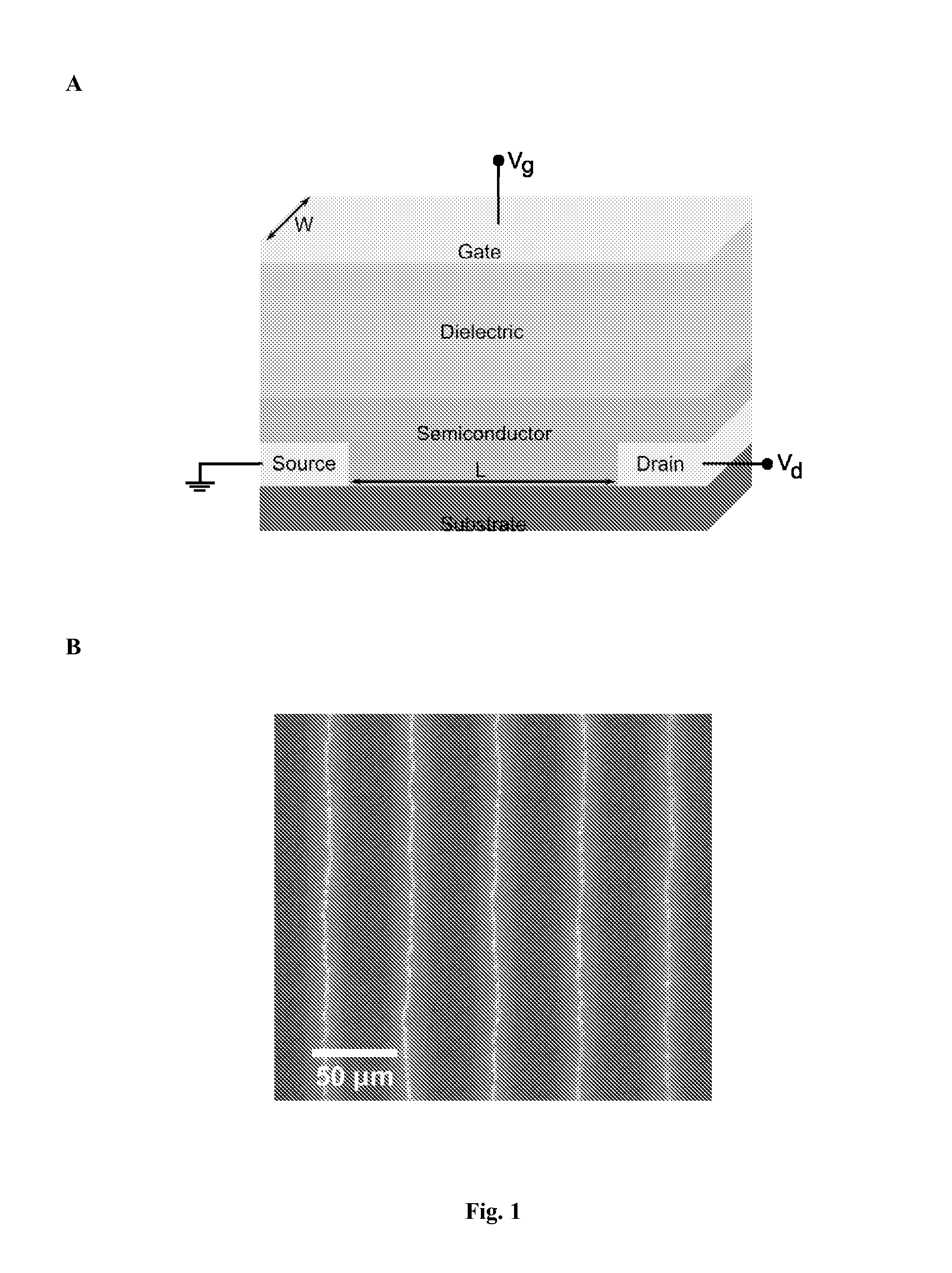
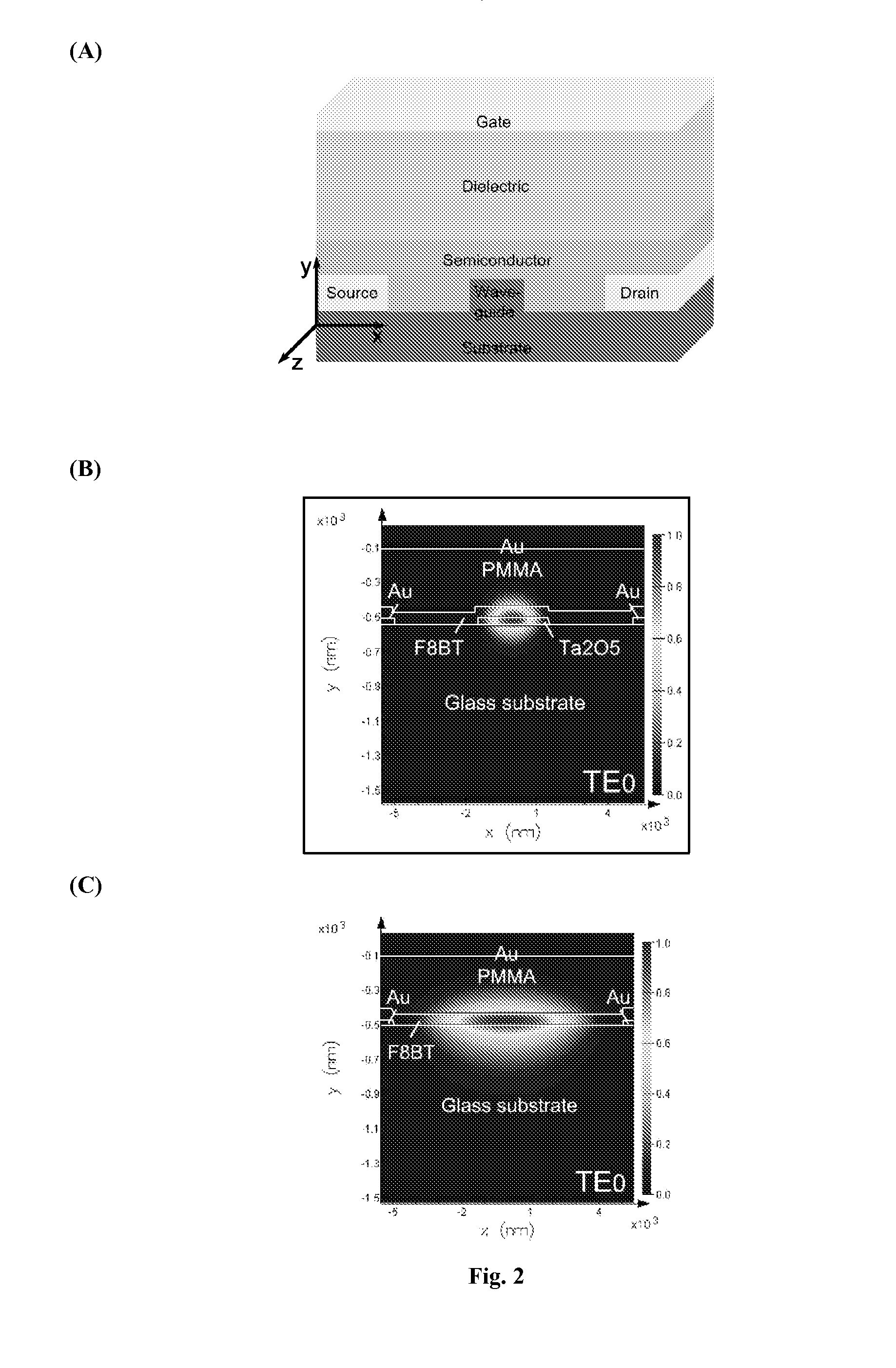
[0040]This invention relates to integrated optoelectronic devices comprising light-emitting field-effect transistors.

[0041]We have recently been able to demonstrate a new optoelectronic device architecture for generating light within ambipolar field-effect transistors. The structure will in the following be referred to as a light-emitting organic field-effect transistor (LFET) (Zaumseil et al, Nature Materials 5, 69 (2006), Zaumseil, et al. Adv. Funct. Materials 18, 2708 (2006), EP 05701898.8), the entire content of which are herewith included in the present application. In an ambipolar LFET, under suitable biasing conditions both electron and hole accumulation layers are simultaneously formed in the channel. At the boundary between the electron and hole accumulation region recombination occurs and emission of light is observed. It is possible to move the recombination zone across the entire channel length by varying the applied biasing conditions. (For example with source=OV, drain...


PUM


Abstract

The present invention relates integrated optoelectronic devices comprising light emitting field-effect transistors. We describe an optoelectronic device comprising a light-emitting field effect transistor (LFET) with an organic semiconductor active layer and a waveguide integrated within the channel of the light-emitting field effect transistor, wherein said waveguide comprises a material which has a higher refractive index than said organic semiconductor. We also describe a light-emitting organic field transistor integrated with a ridge or rib waveguide incorporated within the channel of the LFET; and a similar light-emitting organic field effect transistor in which the waveguide incorporates an optical feedback mechanism.

Description

CROSS REFERENCE TO RELATED APPLICATION[0001]This application is the United States national stage filing of PCT / GB2009 / 051601 entitled “Optoelectronic Devices” and filed Nov. 26 2009; which claims priority to Great Britain Patent Application GB0821980.0 filed Dec. 2, 2008. Each of the aforementioned applications are incorporated herein by reference for all purposes.BACKGROUND OF THE INVENTION[0002]This invention relates to integrated optoelectronic devices comprising light-emitting field-effect transistors.[0003]Organic electronic devices, such as light-emitting diodes, solar cells and field-effect transistors have become of interest for a range of applications in displays and electronics. Organic LEDs have advanced to become one of the most efficient light sources available, organic photodetectors and organic solar cells are capable of near 100% quantum efficiencies, organic-based biological, chemical and mechanical sensors and memory devices are being developed for a range of diffe...

Claims


Application Information

Patent Timeline
Patent Type & Authority Applications(United States)
IPC IPC(8): G02B6/122H01S5/026H01S5/12
CPCH01L51/0545H01L51/0558H01L51/5203H01L51/5275H01S5/36H01S5/12H01S5/187H01S5/22H01S5/3004H01S5/105H01S5/11H10K10/484H10K10/466H10K50/805H10K50/858H01S5/185H10K10/26H10K10/46H10K10/462H10K10/464H10K10/486H10K10/488
Inventor SIRRINGHAUS, HENNINGGWINNER, MICHAEL C.GEISSEN, HARALDSCHWEIZER, HEINZ
Owner CAMBRIDGE ENTERPRISE LTD
Why Eureka
Try Eureka