
Formation of conjugated polymers for solid-state devices

a solid-state device and conjugated polymer technology, applied in the field of electrochromic devices, can solve the problems of poor yield of electrodeposition processes, cost and waste of electrolyte baths,

Active Publication Date: 2011-09-29
UNIV OF CONNECTICUT
View PDF11 Cites 55 Cited by
  • Summary
  • Abstract
  • Description
  • Claims
  • Application Information

AI Technical Summary

Benefits of technology

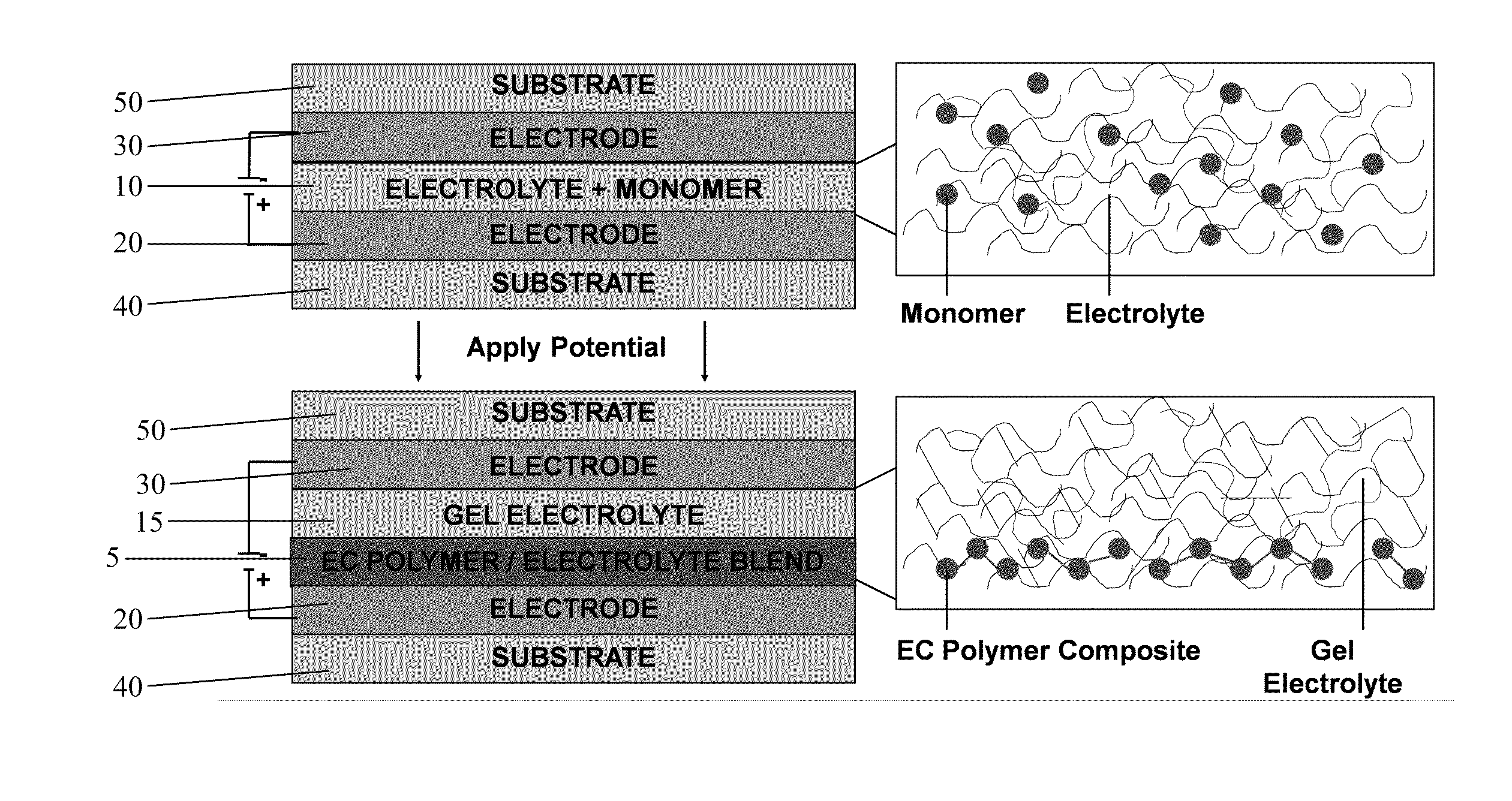
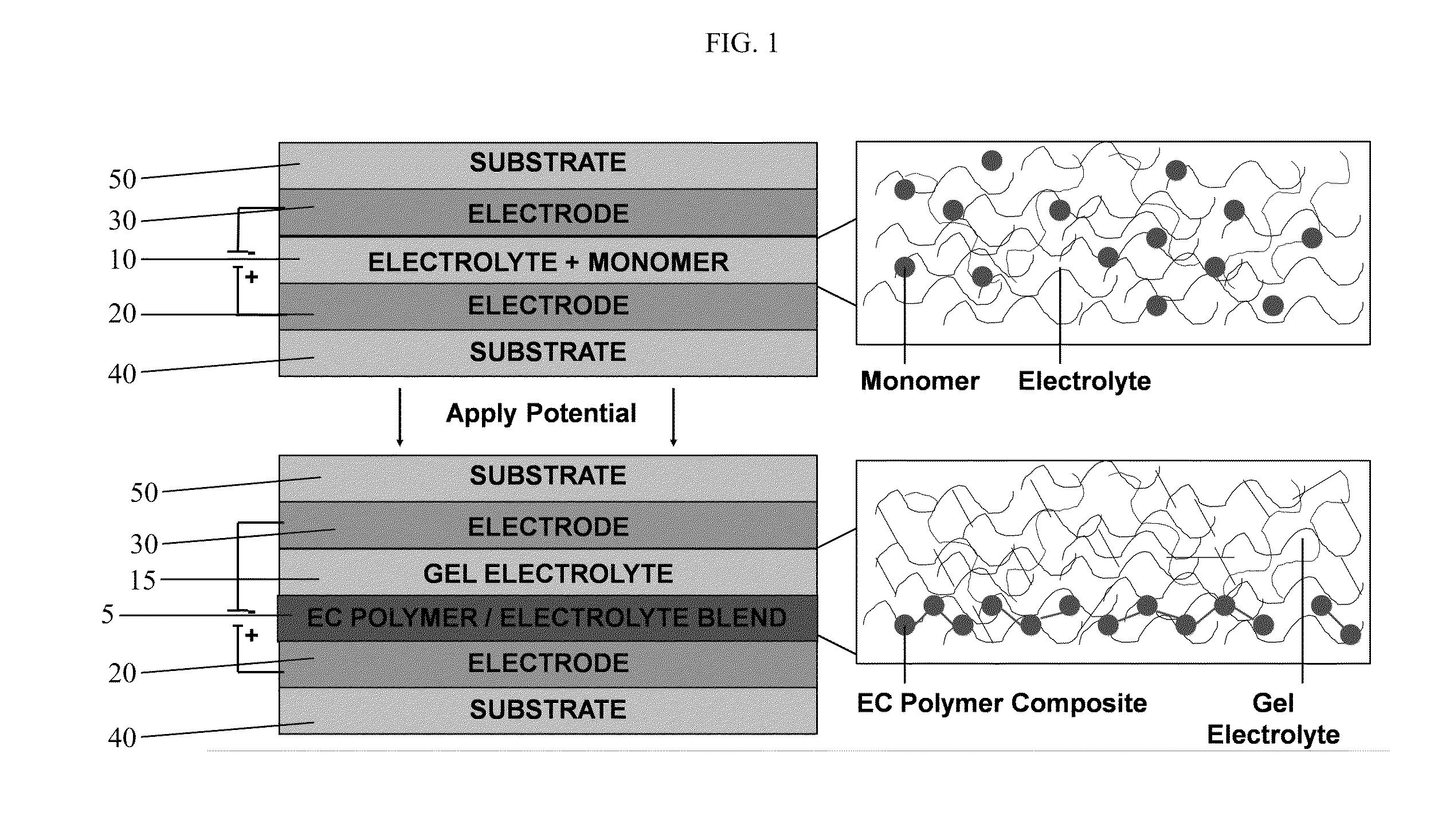
The patent describes a method of making a solid-state device by applying voltage to a device with electrodes and a combination of an electrolyte composition and an electroactive monomer. The electroactive monomer can be polymerized to form a composite of conjugated polymer and electrolyte composition. This method can be used to create solid-state devices with improved performance and stability.

Problems solved by technology

Drawbacks to using electrodeposition include the use of costly and wasteful electrolyte baths, the need for the frequent changing of organic salts and solvents in the baths, as well as the need for proper disposal of spent baths.
Electrodeposition processes are also known to have poor yields.
However, such a process still involved the initial preparation of an electrochromic polymer film prior to device assembly.

Method used


Image

  • Formation of conjugated polymers for solid-state devices
  • Formation of conjugated polymers for solid-state devices
  • Formation of conjugated polymers for solid-state devices

Examples


example 1

In Situ Polymerization of EDOT in an Assembled Solid-State Device

[0127]A device was assembled using a glass / indium-doped tin oxide (ITO) substrate, a polyethylene terephthalate (PET) / ITO substrate, and an electrolyte composition containing 1 gram lithium trifluoromethanesulfonate (LITRIF) salt, 5 grams of polyethylene glycol diacrylate (PEG-DA; Mn=700) as the gel electrolyte precursor, 5 grams of propylene carbonate (PC) plasticizer, and 17.5 milligrams of 2,2;-dimethoxyphenylacetophenone (DMPAP) UV-activated cross-linking agent. To the electrolyte composition was mixed 250 milligrams of 3,4-ethylenedioxythiophene (EDOT) as the electroactive monomer. PEG-DA is crosslinked using UV light 365 nm, 5.8 mW / cm2 for about 15 minutes.

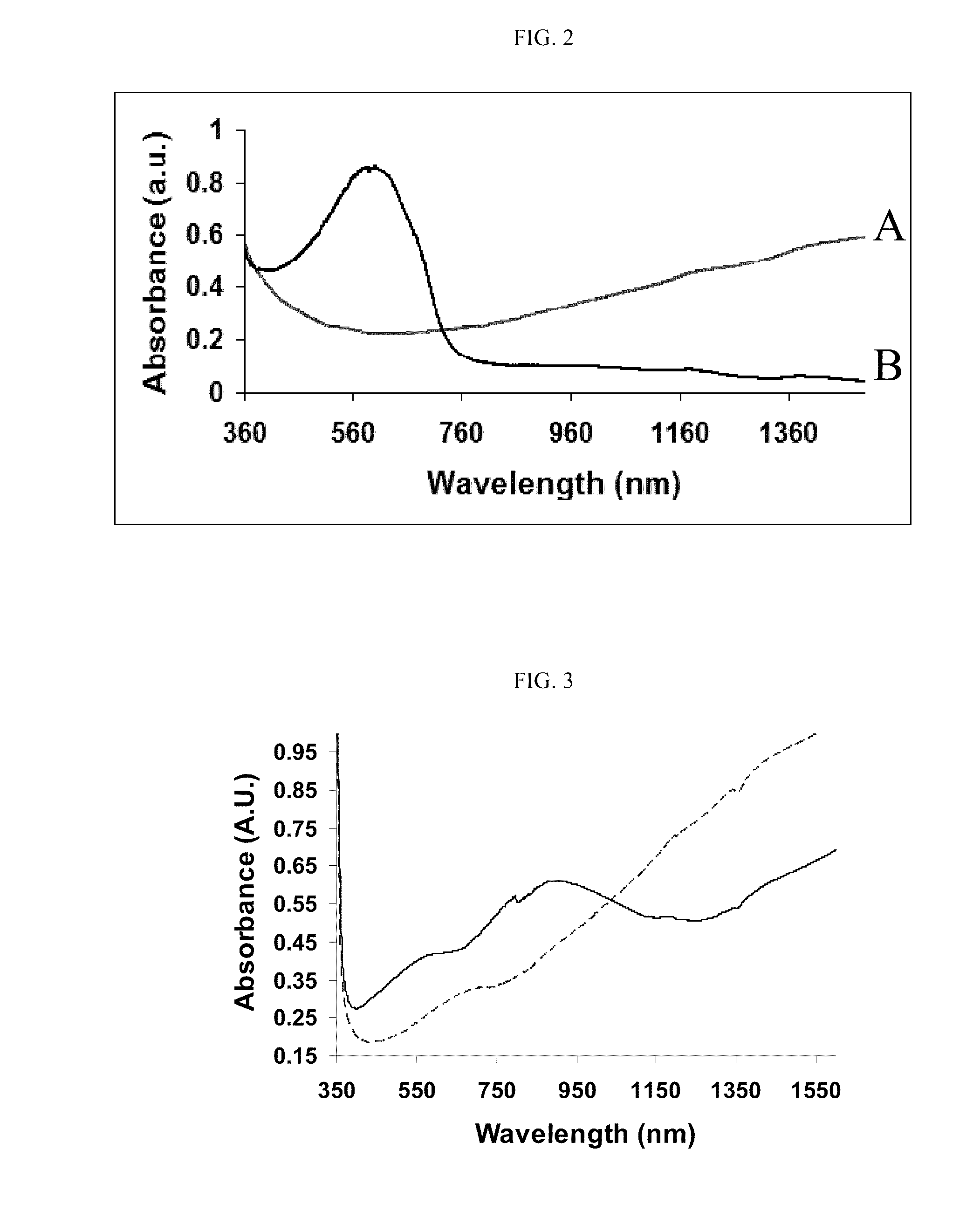
[0128]The device has been shown to switch optically at the same rate as devices prepared with PEDOT films prepared by electrodeposition. Over the course of 50 cycles, no perceived losses had occurred. The CIE Lu′v′ color coordinates for the device containing in...

example 2

In Situ Polymerization of EDOT in an Assembled Solid-State Device using an Ionic Liquid

[0130]A solid-state device similar to Example 1 was prepared using ionic liquid 1-butyl-3-methylimidazolium hexafluorophosphate (BMIMPF6) in the electrolyte composition with no plasticizer component.

example 3

Exploration of the In Situ Polymerization of EDOT in an Assembled Solid-State Device before and after Crosslinking of the Gel Electrolyte Precursor

[0131]Two solid-state devices similar to Example 1 were prepared using no plasticizer. In the first device, the gel electrolyte precursor is crosslinked prior to the in situ polymerization of EDOT. In the second device, a voltage is applied to polymerize EDOT prior to the crosslinking of the gel electrolyte precursor. The second device exhibited a better switching speed (2-5 seconds) and a lower conversion time (30 seconds), while the first device took up to 5 minutes to make a film of PEDOT and exhibits over 25 seconds to switch. It has been shown that the conjugated polymer can be prepared prior to or post crosslinking of the gel electrolyte precursor allowing for more flexible device assembly processes.


PUM

PropertyMeasurementUnit
temperatureaaaaaaaaaa
melting pointsaaaaaaaaaa
wavelengthsaaaaaaaaaa

Abstract

Disclosed herein is a facile process for the formation of conjugated polymers inside or outside assembled solid-state devices. One process generally involves applying a voltage to a device comprising at least two electrodes, a combination of an electrolyte composition and a electroactive monomer disposed between the electrodes, and a potential source in electrical connection with the at least two electrodes; wherein the applying voltage polymerizes the electroactive monomer into a conjugated polymer. Also disclosed are electrochromic articles prepared from the process and solid-state devices comprising a composite of an electrolyte composition and a conjugated polymer.

Description

CROSS REFERENCE TO RELATED APPLICATION[0001]This application claims the benefit of U.S. Provisional Application Ser. No. 61 / 317,457 filed Mar. 25, 2010, which is hereby incorporated by reference in its entirety.TECHNICAL FIELD[0002]The present invention is in the field of electrochromic devices, and more specifically, in the field of electrochromic devices utilizing a conjugated polymer formed inside or outside an assembled solid-state device.BACKGROUND[0003]An electrochromic device is a self-contained, two-electrode (or more) electrolytic cell that includes an electrolyte and one or more electrochromic materials. Electrochromic materials can be organic or inorganic, and reversibly change visible color when oxidized or reduced in response to an applied electrical potential. Electrochromic devices are therefore constructed so as to modulate incident electromagnetic radiation via transmission, absorption, or reflection of the light upon the application of an electric field across the ...

Claims


Application Information

Patent Timeline
Patent Type & Authority Applications(United States)
IPC IPC(8): C25B3/00H01L51/40H01L51/30H10K99/00
CPCC08G2261/3223C08G2261/44C08G2261/54H01L51/0034G02F1/15G02F2001/1515G02F2001/1519C25B3/00G02F1/15165G02F2001/164Y02E10/549H10K85/10H10K85/1135H10K10/46H10K30/00H10K50/11H10K71/125
Inventor SOTZING, GREGORY A.INVERNALE, MICHAEL A.
Owner UNIV OF CONNECTICUT
Learn More