Vertical soi bipolar junction transistor and manufacturing method thereof
a technology of bipolar junction transistor and soi, which is applied in the field of microelectronics and solid-state electronics, can solve the problems of affecting the dc characteristics of the transistor, the inability to easily scale down the lateral soi bjt device, and the limited performance of such devices, and achieves good compatibility and high integration density
- Summary
- Abstract
- Description
- Claims
- Application Information
AI Technical Summary
Benefits of technology
Problems solved by technology
Method used
Image
Examples
first embodiment
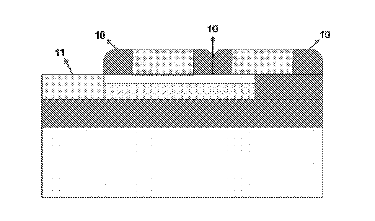
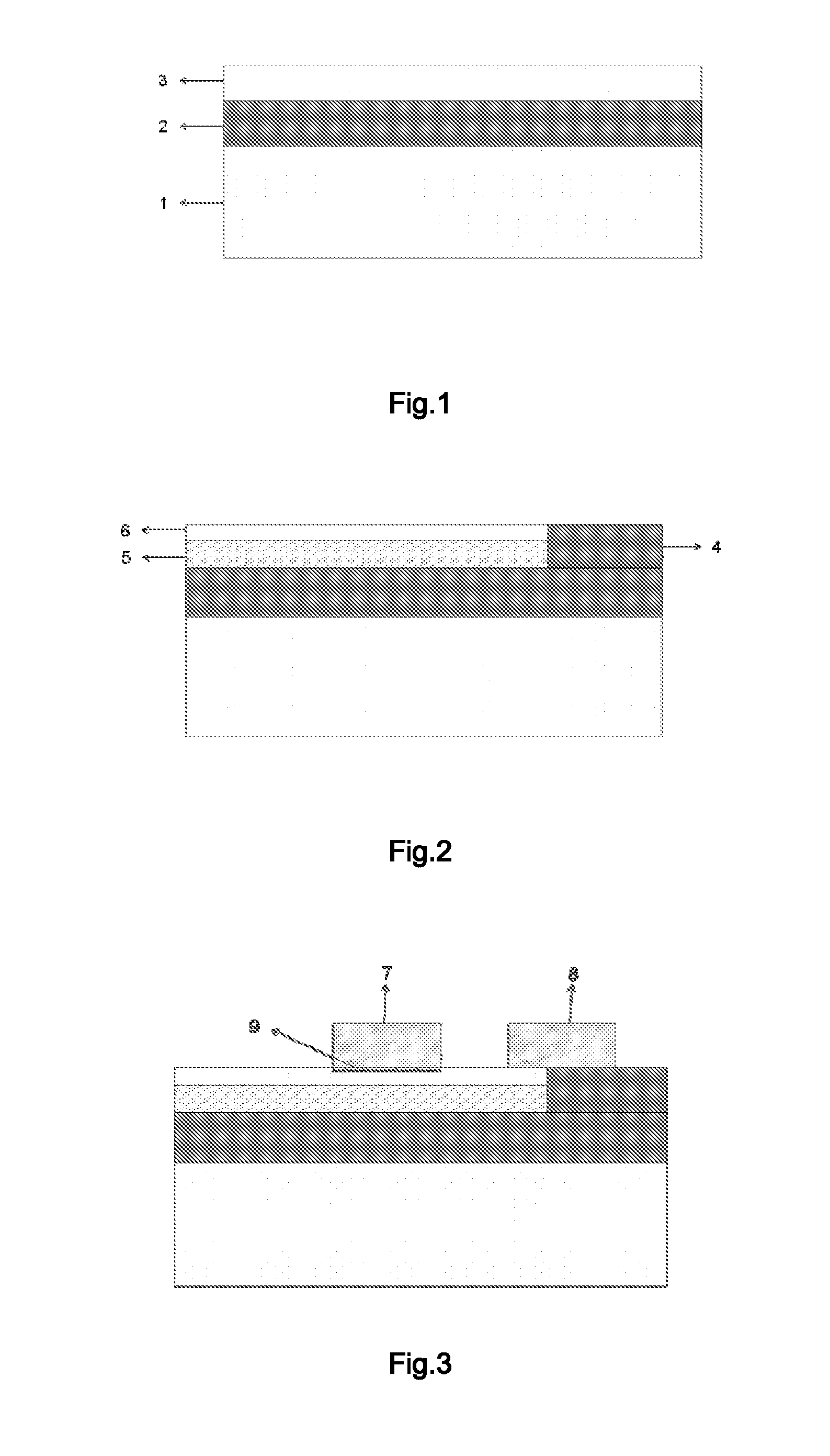
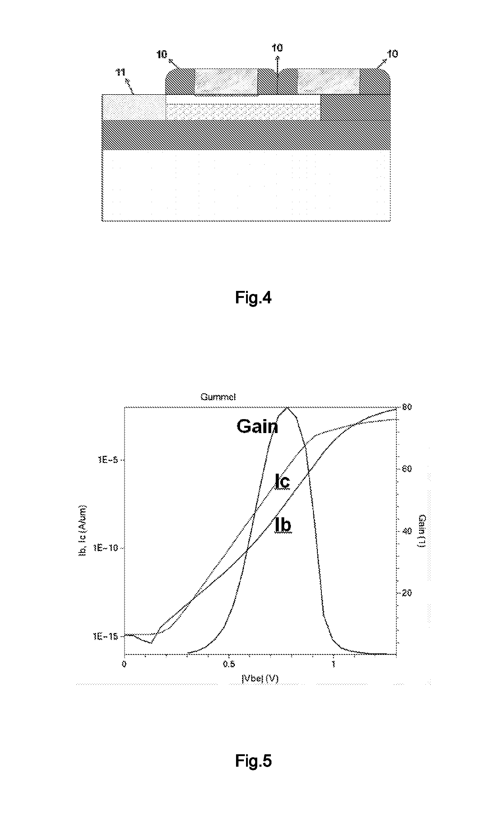
[0037]The present invention relates to a vertical silicon-on-insulator (SOI) bipolar junction transistor (BJT) and a method for manufacturing thereof. Such a vertical SOI BJT realizes a simple double poly silicon technology on SOI. One poly silicon structure means n+ poly silicon emitter which is used for reducing surface recombination velocity of the emitter, so as to improve the emitter injection efficiency and increase the current gain; on the other hand, the impurities in n+ poly silicon emitter can diffuse and form shallow emitter junction. Another poly silicon structure means p+ poly silicon base electrode as a outlet of the base region which can reduce the effective area of the device. According the present invention, the isolation between emitter and base electrode and the isolation between emitter and collector electrode utilize side-wall spacer process in MOS integrated circuit instead normal shallow trench isolation process, which can realize self-alignment, reduce the us...
second embodiment
[0049]The present embodiment provides a NPN type double poly silicon vertical SOI bipolar junction transistor with side-wall spacer and the method for manufacturing thereof.
[0050]The manufacturing method is as follow:
[0051]First, form a SOI BJT active region on an SOI substrate by STI process of integrated circuit.
[0052]Next, a collector region and a base region located in the active region are formed by ion implantation. Wherein, the collector region is formed by doping N-type impurity into the active region with ion implantation process, the doping deep close to the SOI BOX. The base region is formed by implanting P-type impurity into the active region deep close to the surface. The forming of the collector region and the base region adopts a retrograde doping process which has a deep implantation before a shallow implantation. The retrograde doping process can obtain a thinner base region, so as to increase the current gain of transistor, on the other hand, the doping dose of the...
PUM
 Abstract
Description
Claims
Application Information


