

Substrate processing system
- Summary
- Abstract
- Description
- Claims
- Application Information
AI Technical Summary
Benefits of technology
Problems solved by technology
Method used
Image

Examples
Embodiment Construction
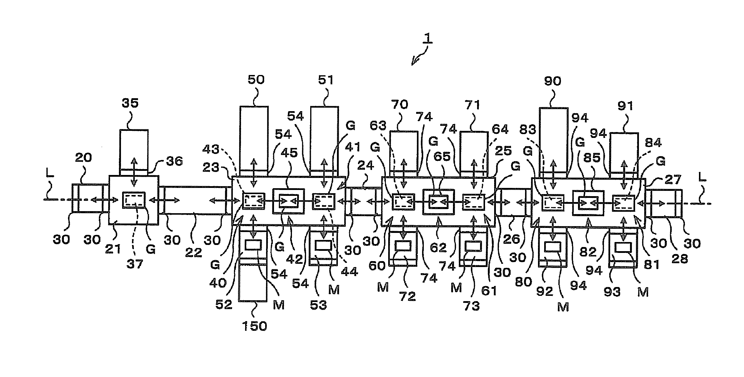
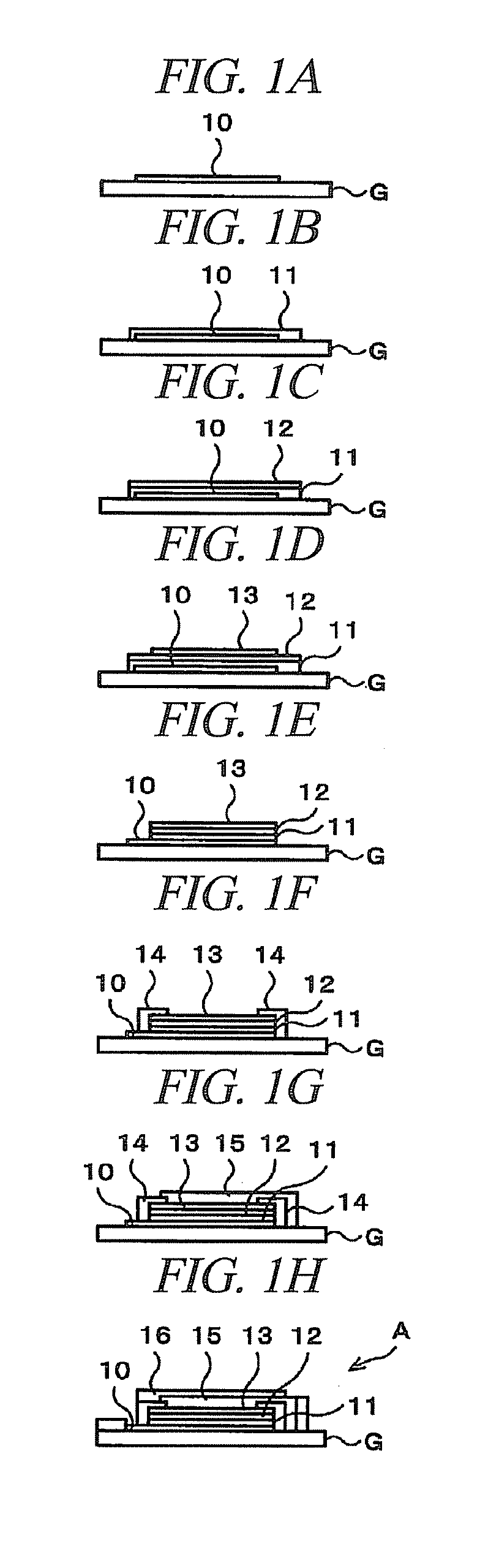
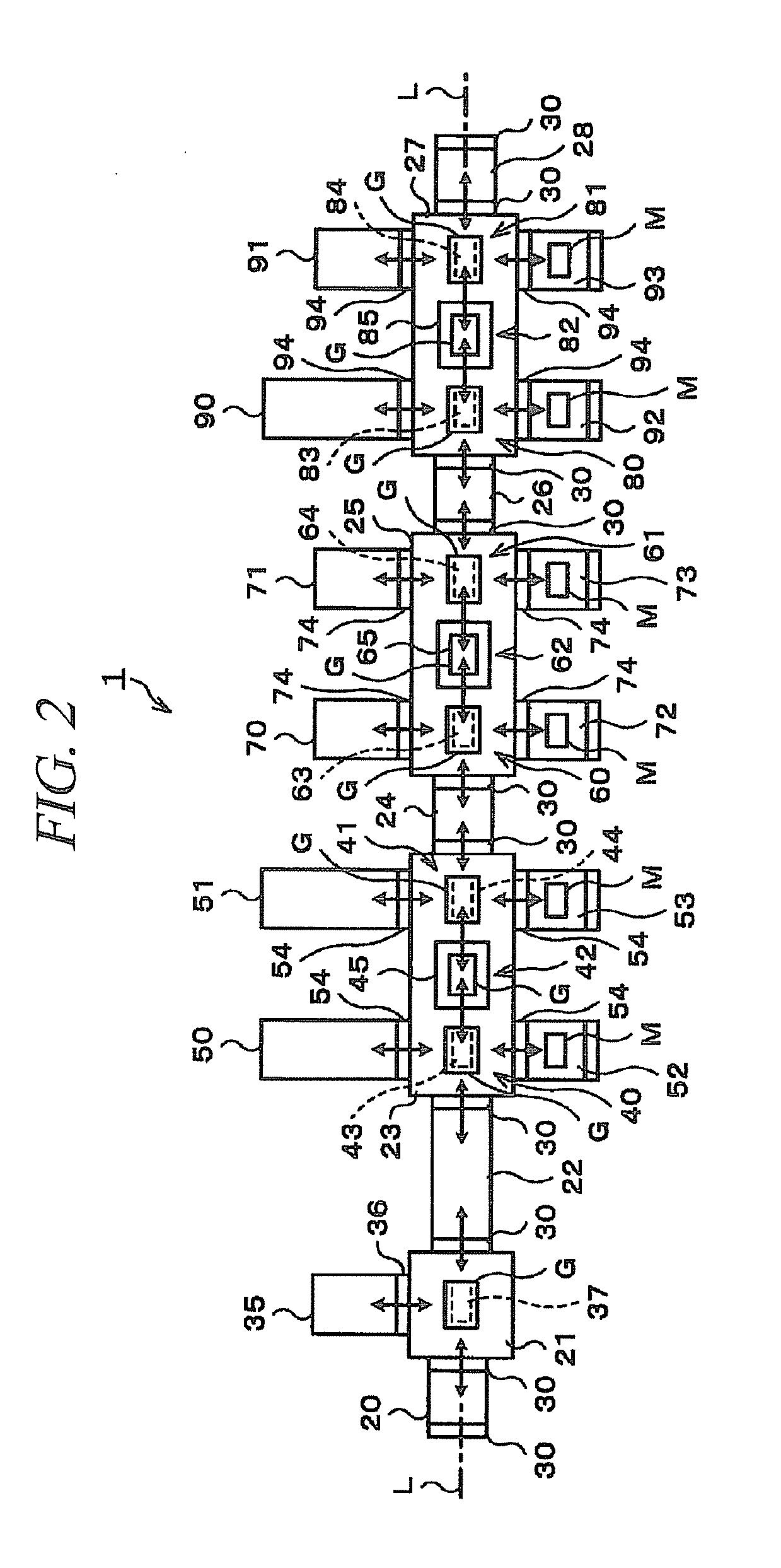
[0061]Hereinafter, embodiments of the present invention will be described in detail with reference to the accompanying drawings. To be specific, in the following embodiments, there will be explained a so-called face-up type substrate processing system 1 capable of manufacturing an organic EL device A by performing a process such as a film forming process onto an upper surface of a substrate G. In the specification and the drawings, elements having substantially the same function are assigned same reference numerals and redundant description thereof may be omitted.
[0062]FIGS. 1A to 1H provide diagrams for explaining a manufacturing process of the organic EL device A in the substrate processing system 1 in accordance with an embodiment of the present invention. As depicted in FIG. 1A, the substrate G on which an anode (positive electrode) layer is formed is prepared. The substrate G is made of a transparent material such as glass. An anode layer 10 is made of a transparent conductive ...
PUM
| Property | Measurement | Unit |
|---|---|---|
| Structure | aaaaa | aaaaa |
| Density | aaaaa | aaaaa |
| Area | aaaaa | aaaaa |
Abstract
Description
Claims
Application Information