Electron beam device and electron beam application device using the same

a technology of electron beam and application device, which is applied in the manufacture of electrode systems, instruments, electric discharge tubes/lamps, etc., can solve the problems of unstable diffusion of schottky electron sources containing barium, and achieve high brightness, wide energy width, and high resolution

Active Publication Date: 2011-10-06
HITACHI HIGH-TECH CORP
View PDF22 Cites 28 Cited by
  • Summary
  • Abstract
  • Description
  • Claims
  • Application Information

AI Technical Summary

Benefits of technology

[0016]The configurations allow an SE electron source to maintain a monochromatic and high-brightness region and to maintain high brightness without broadening the energy width e

Problems solved by technology

The Schottky electron source containing barium

Method used


Image

  • Electron beam device and electron beam application device using the same
  • Electron beam device and electron beam application device using the same
  • Electron beam device and electron beam application device using the same

Examples


embodiment 1

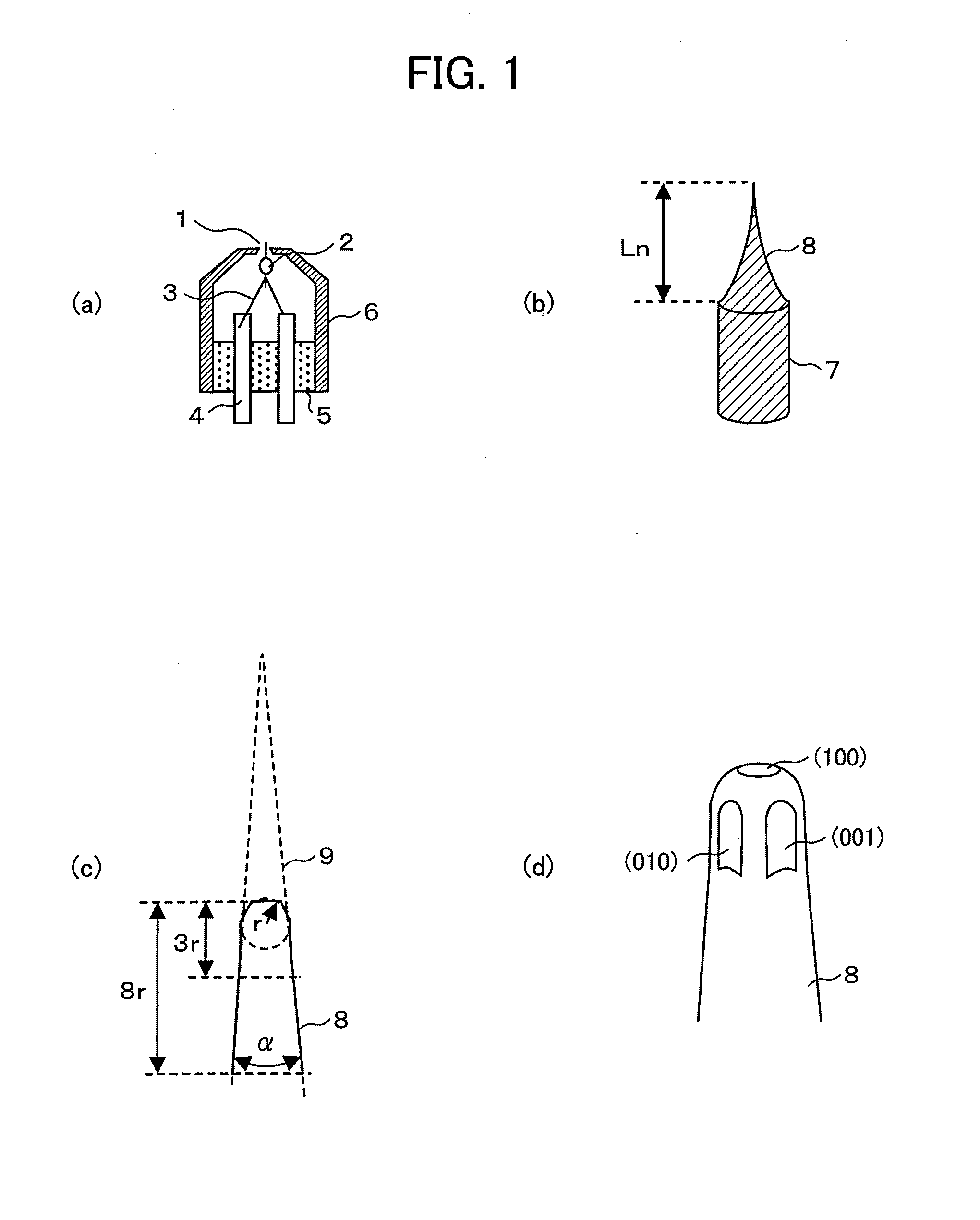
[0029]FIG. 1 depicts an electron beam application apparatus as an embodiment of the present invention.

[0030]The electron beam application apparatus illustrated in FIG. 1(a) includes a tungsten needle 1, as well as a heater 3 and a Zr—O diffusion source 2 both supporting the tungsten needle 1. The tungsten needle 1 serves as an electron emission source. The heater 3 is composed of tungsten filaments. These components are held on an insulator 5 and electrodes 4 and are covered by a suppressor 6 which suppresses thermal electrons. With reference to FIG. 1(b), the tungsten needle (single-crystal tungsten metal needle) 1 has a needle-shaped tip 8. The needle-shaped tip 8 is a portion (this portion is hereinafter temporarily referred to as “constricted region”) extending from a cylindrical portion of the single-crystal tungsten rod to the tip. The needle-shaped tip 8 has a length Ln of preferably 200 μm or less for maintaining the strength of the needle and providing a suitably short diff...

embodiment 2

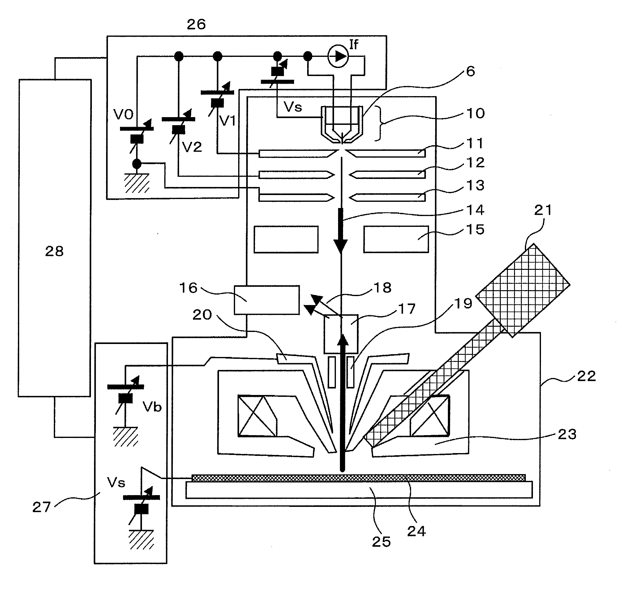
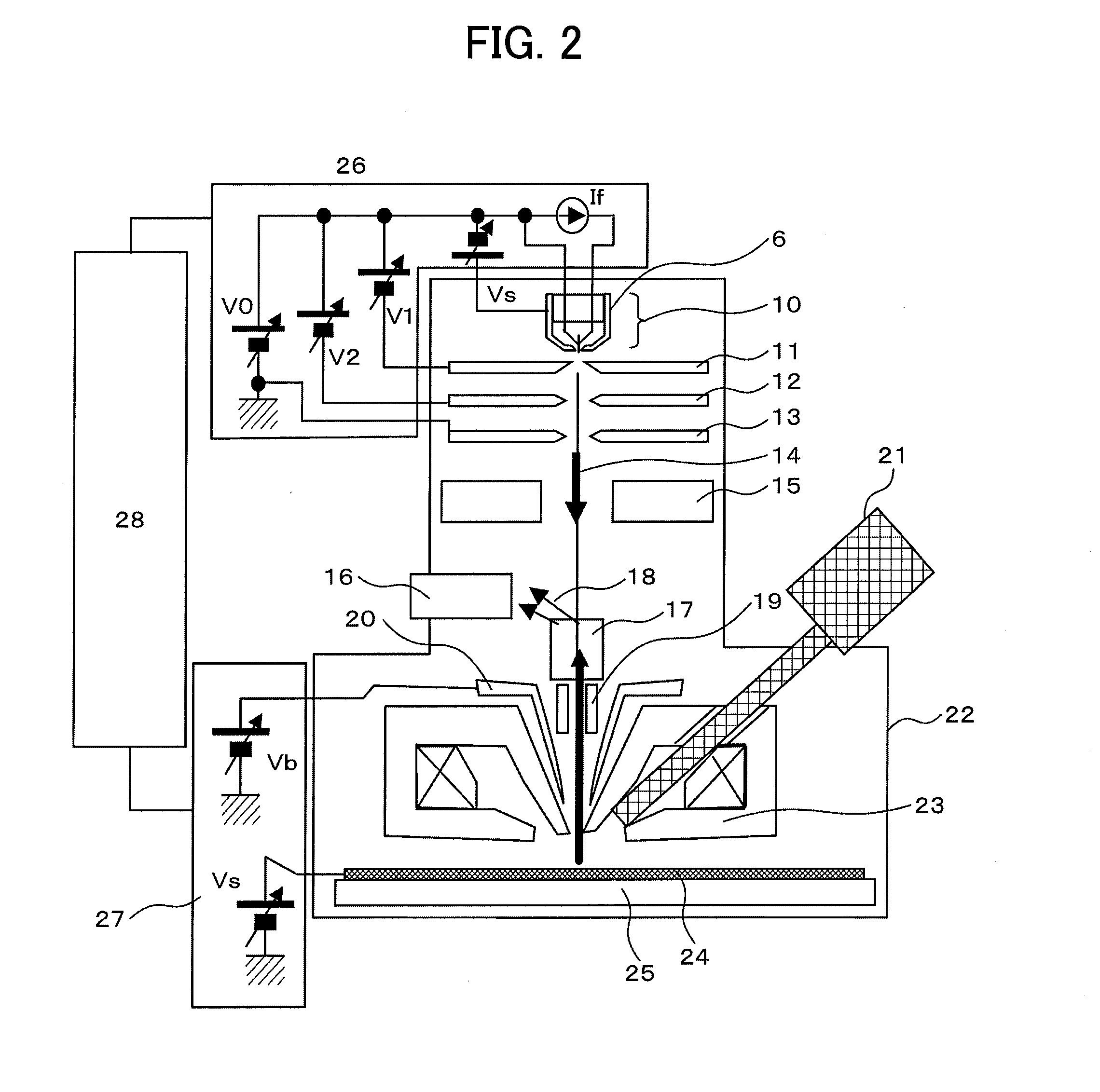
[0057]FIG. 8(a) shows an electron source according to another embodiment of the present invention. A portion which emits electrons is a needle-shaped tip 8 arranged at the tip of a single-crystal tungsten rod 7. By energizing a tungsten filament heater 104 for heating, an oxide containing Ba—O migrates from a diffusion source 102 and is impregnated into a metal sintered body 100. These components are housed in a cathode support tube 105, over which a cathode cap 106 is installed both to prevent the metal sintered body 100 from dropping off and to control the oxygen partial pressure. The metal sintered body 100 contains tungsten as a principal component, and barium and oxygen atoms, which are formed through reduction by tungsten, diffuse through the surface of the single-crystal tungsten rod and form a low-work-function surface of Ba—O—W at the needle-shaped tip 8, from which electron beams are emitted. Power is supplied to the heater 104 via two electrodes 4.

[0058]To supply a curren...


PUM


Abstract

To obtain a SEM capable of both providing high resolution at low acceleration voltage and allowing high-speed elemental distribution measurement, a SE electron source including Zr—O as a diffusion source is shaped so that the radius r of curvature of the tip is more than 0.5 μm and less than 1 μm, and the cone angle α of a conical portion at a portion in the vicinity of the tip at a distance of 3r to 8r from the tip, is more than 5° and less than (8/r)°. Another SE electron source uses Ba—O and includes a barium diffusion supply means composed of a sintered metal and a barium diffusion source containing barium oxide.

Description

TECHNICAL FIELD[0001]The present invention relates to an electron beam apparatus and an electron beam application apparatus using the same, which electron beam apparatus has functions such as high resolution analysis at low acceleration voltage and elemental analysis at high speed at a large current. Specifically, the present invention relates to a scanning electron microscope (SEM) for the observation of microstructures using electron beams.BACKGROUND ART[0002]A Schottky emission electron source (hereinafter also briefly referred to as “SE electron source”) is used in scanning electron microscopes (SEM) with a high resolution at low acceleration voltage and electron irradiation apparatuses for element analyses at high speed with X rays, because the SE electron source gives monochromatic, highly bright electron beams and easily provides a large probe current . This electron source includes a single-crystal tungsten (100) rod having a diameter of about 0.1 mm, the tip (apex) of the r...

Claims


Application Information

Patent Timeline
IPC IPC(8): H01J9/02H01J19/02H01J37/073
CPCH01J37/065H01J37/075H01J2237/06316H01J37/28H01J37/256
Inventor OHSHIMA, TAKASHITOMIMATSU, SATOSHI
Owner HITACHI HIGH-TECH CORP
Why Eureka
Try Eureka