ADC

a digital converter and analog technology, applied in the field of analogtodigital converters, can solve the problems of reducing the input bandwidth even further, and limiting the bandwidth, so as to achieve significant power advantages, improve the speed of operation, and increase the degree of design freedom

Active Publication Date: 2011-10-06
NXP BV
View PDF2 Cites 27 Cited by
  • Summary
  • Abstract
  • Description
  • Claims
  • Application Information

AI Technical Summary

Benefits of technology

[0021]In an alternative, non-limiting embodiment, the signal selector unit is connected between the pre-conditioning unit and the ADC unit, and the ADC further comprises a second pre-processor unit. Such an ADC may be a time-interleaved ADC and the ADC unit may be a successive approximation register ADC unit. This embodiment is particularly advantageous in that it offers a better speed of operation, than other embodiments, particularly for those cases where the speed limitation comes from the long feedback path.
[0022]Beneficially, in addition to the linearity improvements that may result from embodiments of the invention, embodiments of the invention can result in more degrees of design freedom for the amplifier requirements: since there is no longer the need to satisfy linearity within the amplifier, the design optimization need consider only bandwidth and voltage headroom. This in return brings a significant power advantage compared to an optimization where linearity is taken into account, and thereby allows the Time Interleaved converter to reach higher speed.

Problems solved by technology

Because all SAR ADC's process the same input signal, the distribution of the input signal from the input source via the high-speed T / H to each individual SAR ADC inputs creates a significant interconnection wire overhead, leading to bandwidth limitations.
It can also create different signal delays from one SAR ADC unit to the other, which reflect to performance degradation.
Capacitive loading of the SAR ADC input stages reduce the input bandwidth even further.
The problem just described becomes a performance-limiting factor in modern submicron CMOS processes (e.g. 65 nm) with low supply voltages.
It becomes increasingly difficult in these processes to realize such buffers that offer broad signal bandwidth (e.g. GHz), very high linearity (e.g. Total-Harmonic-Distortion of −60 dB, or less) and high signal swing (e.g. 0.5-1V), the last being required to reduce the noise impact on the signal quality.

Method used


Image

  •  ADC
  •  ADC
  •  ADC

Examples


Embodiment Construction

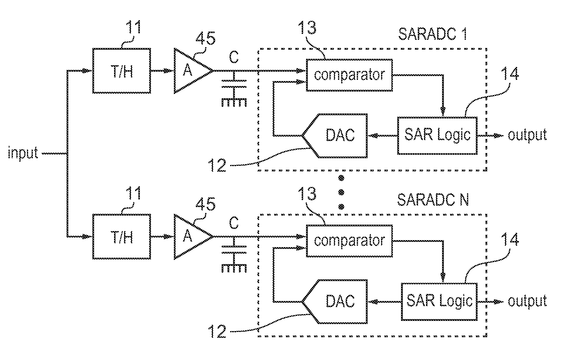
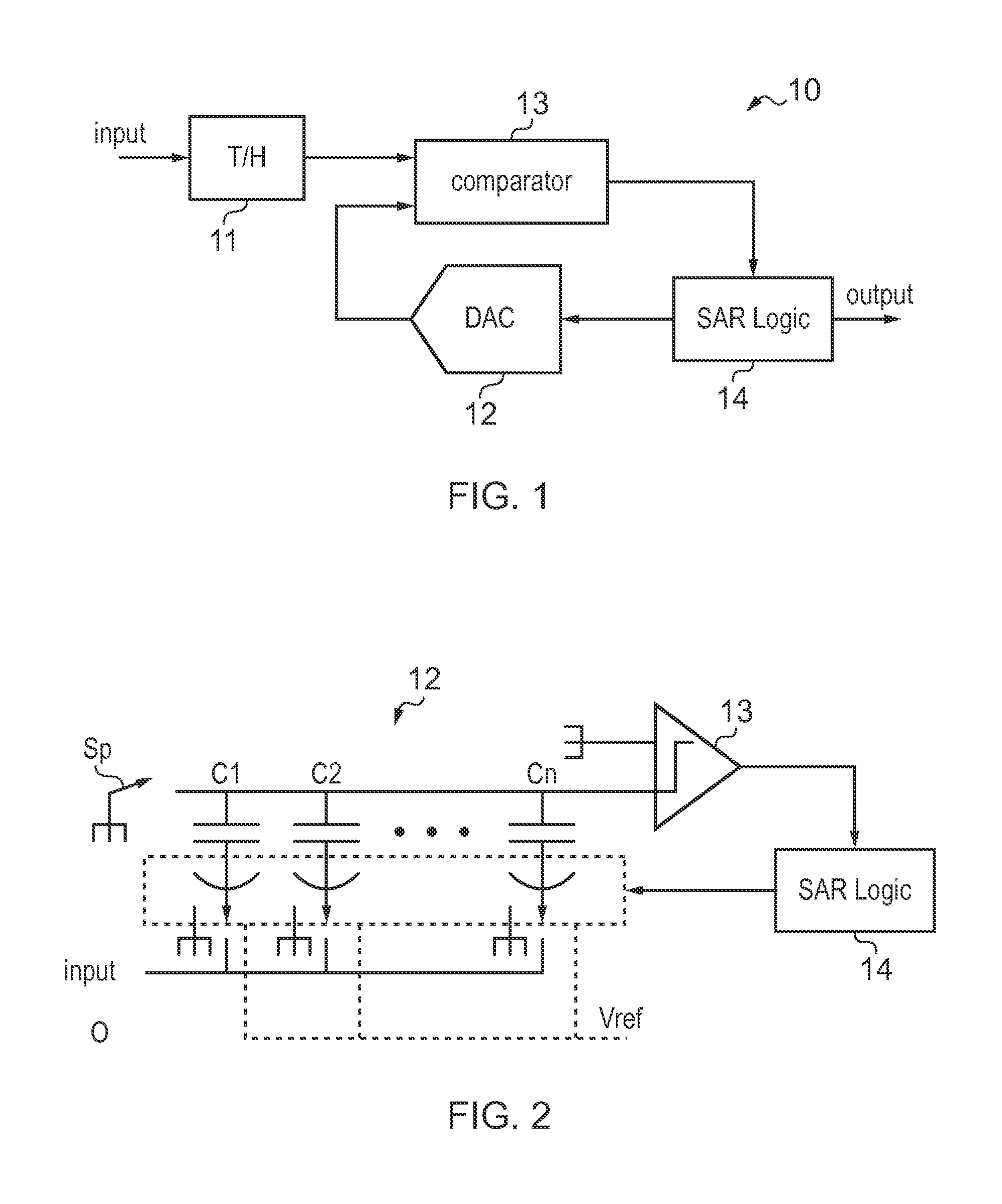
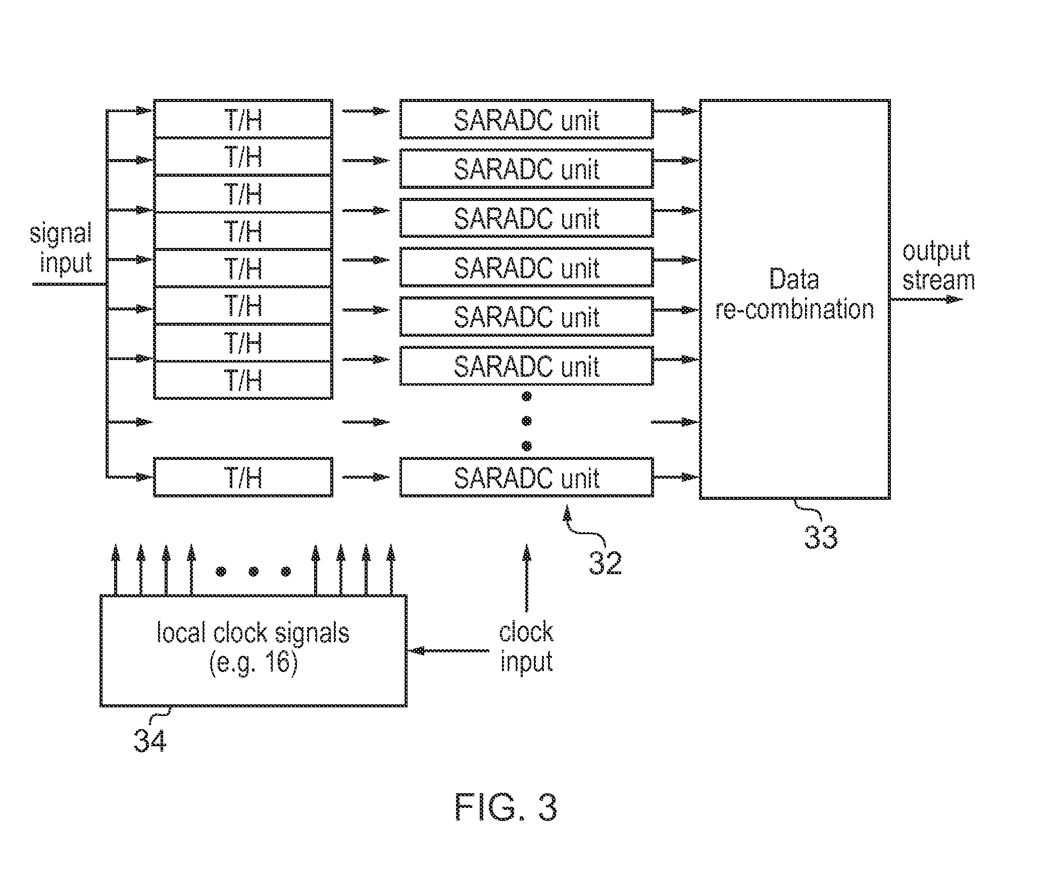
[0039]In order to aid an understanding of the invention, it will be helpful to consider a source of inaccuracies which ADCs according to embodiment of the invention can reduce or ameliorate: in signal processing systems such as Analog-to-Digital converters, main signal processing devices 52 such as the one shown in FIG. 5 form basic parts of conversion algorithms processing a multiplicity of input signals x, y, . . . to generate signal z. A comparator is an example of a main processing device comparing signals x and y and generating the result z.

[0040]Often, signals x and y have significantly different electrical properties, e.g. common mode level, or the circuits that generate them cannot directly interface with the main processing device. In these cases, these signals must be pre-conditioned before being processed by the main device. This is shown in FIG. 5, assuming that signal x requires pre-conditioning by pre-conditioner 51 resulting in x′. Signal x′, instead of x, will now be...


PUM


Abstract

This invention relates to Analog to Digital Converters (ADC) and, inter alia, to Time Interleaved ADCs and Successive Approximation Register (SAR) ADC's. In a conventional Time Interleaved ADC employing SAR ADC units, the input signal is processed through a track-and-hold circuit (T/H), and then through a buffer circuit, before the SAR ADC unit. There, by means of a comparator, the signal is compared with a Digital-to-Analog Converter (DAC) signal from the SAR logic. The buffer reduces the influence of capacitive loading and physical layout design on the SAR ADC input, but typically has a non-linear response and thus introduces distortion to the input signal. This can limit the ADC linearity, particularly for high-speed ADCs operating with low-supply voltages. An objective of the invention is to reduce or eliminate the effect of the buffer non-linearity. This is done in some embodiments by routing both the signals to the comparator through the same buffer circuit. In another embodiment the DAC signal is routed through a separate second buffer circuit. By use of a single buffer circuit, or where there is ideal matching of the buffer circuits in the latter embodiment, the distortion effects are completely eliminated; however, for practical imperfectly matched buffer circuits according to the latter embodiment, the gain and off-set mismatches can be accommodated through calibration of the buffers or, in suitable applications, through the DAC calibration.

Description

FIELD OF THE INVENTION[0001]This invention relates to Analog-to-Digital Converters (ADC), and in particular to ADCs which comprise pre-conditioning units such as buffersBACKGROUND OF THE INVENTION[0002]An ADC 10 is shown in FIG. 1. This example ADC is a Successive Approximation Register ADC (SAR-ADC). The ADC input is connected to a track-and-hold unit 11. A comparator 13 compares the input held in the track-and-hold unit 11 with the value output from a Digital-to-Analog Converter (DAC) 12. The comparator output is input to the SAR logic 14, which provides both the ADC output and the input to the DAC 12.[0003]The converter works with the binary search algorithm. First, the input signal is applied and compared with half the scale of the signal reference (thus, the 100..00). Dependent on the comparison result, the DAC output value is increased or reduced in binary levels to approximate successively the input signal. For a 10 bit (10b) SAR ADC, a minimum of 10 successive cycles is need...

Claims


Application Information

Patent Timeline
Patent Type & Authority Applications(United States)
IPC IPC(8): H03M1/00
CPCH03M1/0614H03M1/466H03M1/1215
Inventor DORIS, KONSTANTINOSJANSSEN, ERWIN
Owner NXP BV
Why Eureka
Try Eureka