Solid-state image pickup apparatus signal processing method for a solid-state image pickup apparatus, and electronic apparatus

a solid-state image and pickup apparatus technology, applied in the direction of diodes, color television details, television systems, etc., can solve the problems of small reduced ad convertible input voltage range, and not only the dispersion of reset levels, so as to reduce the input voltage range within which the input voltage can be processed by the signal processing section, the effect of reducing the output amplitude of the pixel

Inactive Publication Date: 2011-10-06
SONY CORP
View PDF2 Cites 62 Cited by
  • Summary
  • Abstract
  • Description
  • Claims
  • Application Information

AI Technical Summary

Benefits of technology

[0035]With the solid-state image pickup apparatus, since the voltage is set using a signal of a pixel of a processing object, such a great difference in in-plane fluctuation of a characteristic or an in-plane distribution and an offset component which depends upon the magnitude of parasitic capacitance as in the ca

Problems solved by technology

However, the reset level suffers not only from a dispersion among different unit pixels arising from a threshold dispersion of an amplification transistor and so forth but also from a difference by a great spatial fluctuation of a characteristic in a plane in a two-dimensional array of the unit pixels, that is, by an in-plane distribution or from a time-dependent variation by the temperature variation upon operation.
In the case where a fixed voltage is applied as

Method used


Image

  • Solid-state image pickup apparatus signal processing method for a solid-state image pickup apparatus, and electronic apparatus
  • Solid-state image pickup apparatus signal processing method for a solid-state image pickup apparatus, and electronic apparatus
  • Solid-state image pickup apparatus signal processing method for a solid-state image pickup apparatus, and electronic apparatus

Examples


first embodiment

1. First Embodiment

1-1. System Configuration

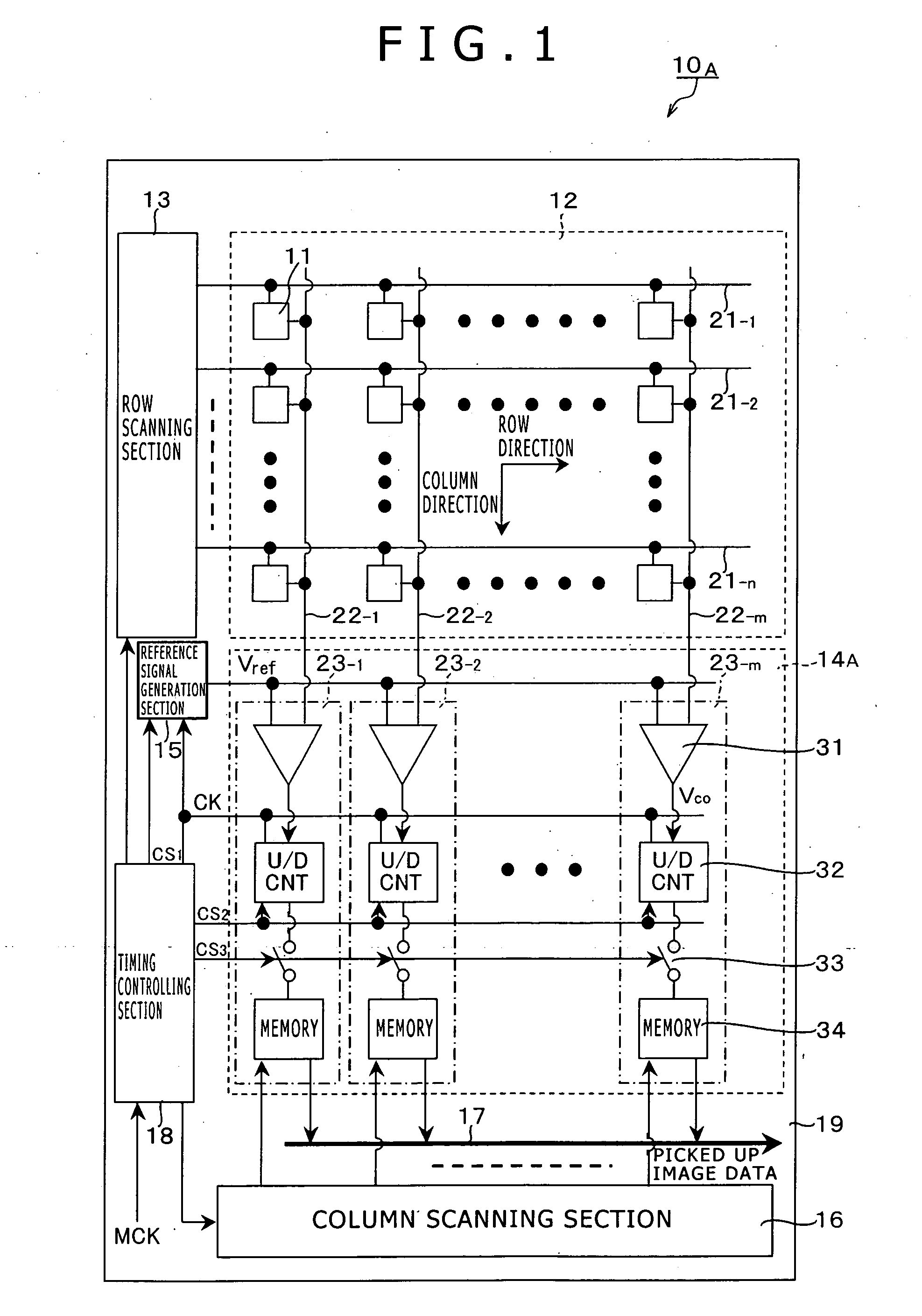
[0098]FIG. 1 shows a general configuration of a solid-state image pickup apparatus according to a first embodiment of the present invention, for example, a complementary metal oxide semiconductor (CMOS) image sensor which is a kind of X-Y address type solid-state image pickup apparatus. The CMOS image sensor is an image sensor produced applying a CMOS process or partially using a CMOS process.

[0099]Referring to FIG. 1, the CMOS image sensor 10A according to the present embodiment includes a pixel array section 12 having a plurality of unit pixels 11 disposed two-dimensionally in rows and columns, and peripheral driving and signal processing systems for driving the unit pixels 11 of the pixel array section 12. In the CMOS image sensor 10A shown in FIG. 1, as the peripheral driving and signal processing systems, for example, a row scanning section 13, a column processing section 14A, a reference signal generation section 15, a column scannin...

working example 3

[0210]FIG. 19 is a circuit diagram showing an example of a configuration of a comparator according to a working example 3 which includes a function for adjusting the internal reference voltages Vouti and Vrefi of the AD conversion circuit 23.

[0211]Referring to FIG. 19, the comparator 31C according to the working example 3 has a two-stage circuit structure including a preceding stage circuit section and a succeeding stage circuit section. The preceding stage circuit section has a circuit configuration same as that of the comparator 31A according to the working example 1, that is, has a circuit configuration of a comparison circuit section 81. It is to be noted that the preceding stage circuit section is not limited to that of a circuit configuration same as that of the comparator 31A according to the working example 1, but may have a circuit configuration same as that of the comparator 31B according to the working example 2.

[0212]On the other hand, the succeeding stage circuit sectio...

first driving example

[0216]Now, a first driving example of the comparator 31C according to the working example 3 which includes the storage circuit section 82 on the succeeding stage of the comparison circuit section 81 is described with reference to a timing waveform diagram of FIG. 20. In FIG. 20, timing waveforms of the control signals xΦR, xΦext and xΦR2, reference voltages Vrefi, Vouti are illustrated.

[0217]First, upon CDS driving, in the comparison circuit section 81, an initial voltage set by placement of the PMOS transistors 58 and 59 into a conducting state is retained as the internal reference voltages Vouti and Vrefi into the gate side of the NMOS transistors 51 and 52 under the control of the control signal xΦR. In the initialization state, NMOS transistor 823 of the storage circuit section 82 on the succeeding stage is placed into a conducting state under the control of the control signal xΦR2.

[0218]When the NMOS transistor 823 in the storage circuit section 82 on the succeeding stage is pl...


PUM


Abstract

Disclosed herein is a solid-state image pickup apparatus, including a pixel array section in which a unit pixel including a photoelectric conversion section and a charge detection section for detecting charge generated by photoelectric conversion by the photoelectric conversion section is disposed; a driving section adapted to carry out driving of reading out a signal of the unit pixel divisionally by twice as a first signal and a second signal; and a signal processing section adapted to set the first signal read out first from the unit pixel as a reference voltage for a processable input voltage range of the signal processing section, adjust the reference voltage so that the first and second signals may be included in the input voltage range and carry out signal processing for the first and second signals using the adjusted reference voltage.

Description

BACKGROUND OF THE INVENTION[0001]1. Field of the Invention[0002]This invention relates to a solid-state image pickup apparatus, a signal processing method for a solid-state image pickup apparatus, and an electronic apparatus.[0003]2. Description of the Related Art[0004]A solid-state image pickup apparatus is known which includes a unit pixel which in turn includes a photoelectric conversion section, a charge detection section and a transfer gate section for transferring charge accumulated in the photoelectric conversion section to the charge detection section. A solid-state image pickup apparatus of the type described usually carries out a noise removing process by correlation double sampling in order to remove noise upon a resetting operation. In the following description, the charge detection section is referred to as FD (Floating Diffusion) section. As a method of the noise removing process, a method which uses digital signal processing and another method which uses analog signal...

Claims


Application Information

Patent Timeline
IPC IPC(8): H04N5/335
CPCH04N5/355H04N5/335H04N5/378H04N5/3575H04N25/57H04N25/616H04N25/75H01L27/14643H04N25/60H04N25/65H04N25/709H04N25/00H04N25/67H04N25/77
Inventor SAKAKIBARA, MASAKITAURA, TADAYUKIOIKE, YUSUKETAKATSUKA, TAKAFUMIKATO, AKIHIKO
Owner SONY CORP
Why Eureka
Try Eureka