Reverse conducting IGBT

a reverse conducting, bipolar transistor technology, applied in the direction of transistors, semiconductor devices, electrical apparatus, etc., can solve the problems of additional testing time, increased material costs, and associated cost of the package, and achieves the effect of simple and cost-effectiv

Inactive Publication Date: 2011-10-20
SINOPOWER SEMICON
View PDF1 Cites 30 Cited by
  • Summary
  • Abstract
  • Description
  • Claims
  • Application Information

AI Technical Summary

Benefits of technology

[0011]It is an object of the present invention to provide a simple and cost effective RC-IGBT design which at least mitigates the above trade-off.

Problems solved by technology

This results in additional BOM (Bill of Material), additional testing time, and increased cost for the separate devices, and associated cost for the package.
Moreover the approach of co-packing the IGBT and diode in one package increases the probable yield loss of the module, as failure of any of these devices results in malfunction of the whole part.
This leads to insulation, chip displacement and wiring issues for the package.
In addition, this also results in a parasitic inductance which restrains the switching speed of the IGBT.
The first is that there is an undesirable snapback characteristic realised when the IGBT is in a forward mode.
This snapback characteristic has a negative resistance associated with it which produces harmonics and can lead to undesirable ringing and oscillations in the system.
It has been demonstrated that, by reducing the area density of the N+ regions compared to the P+ anode region, it is possible to reduce the snapback characteristic but at the expense of a poorer performance of the anti-parallel diode in the reverse mode (that is the conduction through the IGBT).

Method used


Image

  • Reverse conducting IGBT
  • Reverse conducting IGBT
  • Reverse conducting IGBT

Examples


Embodiment Construction

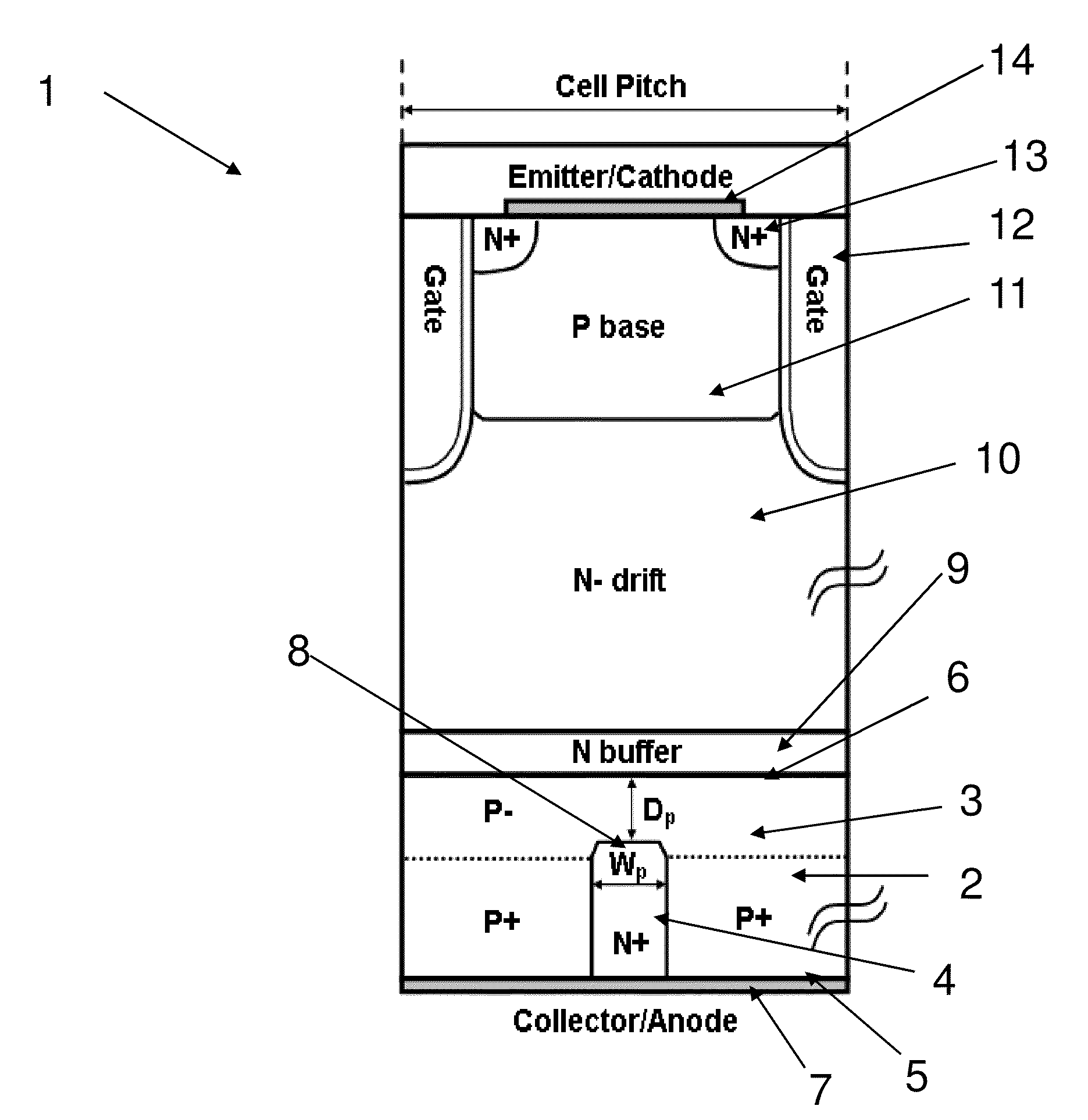
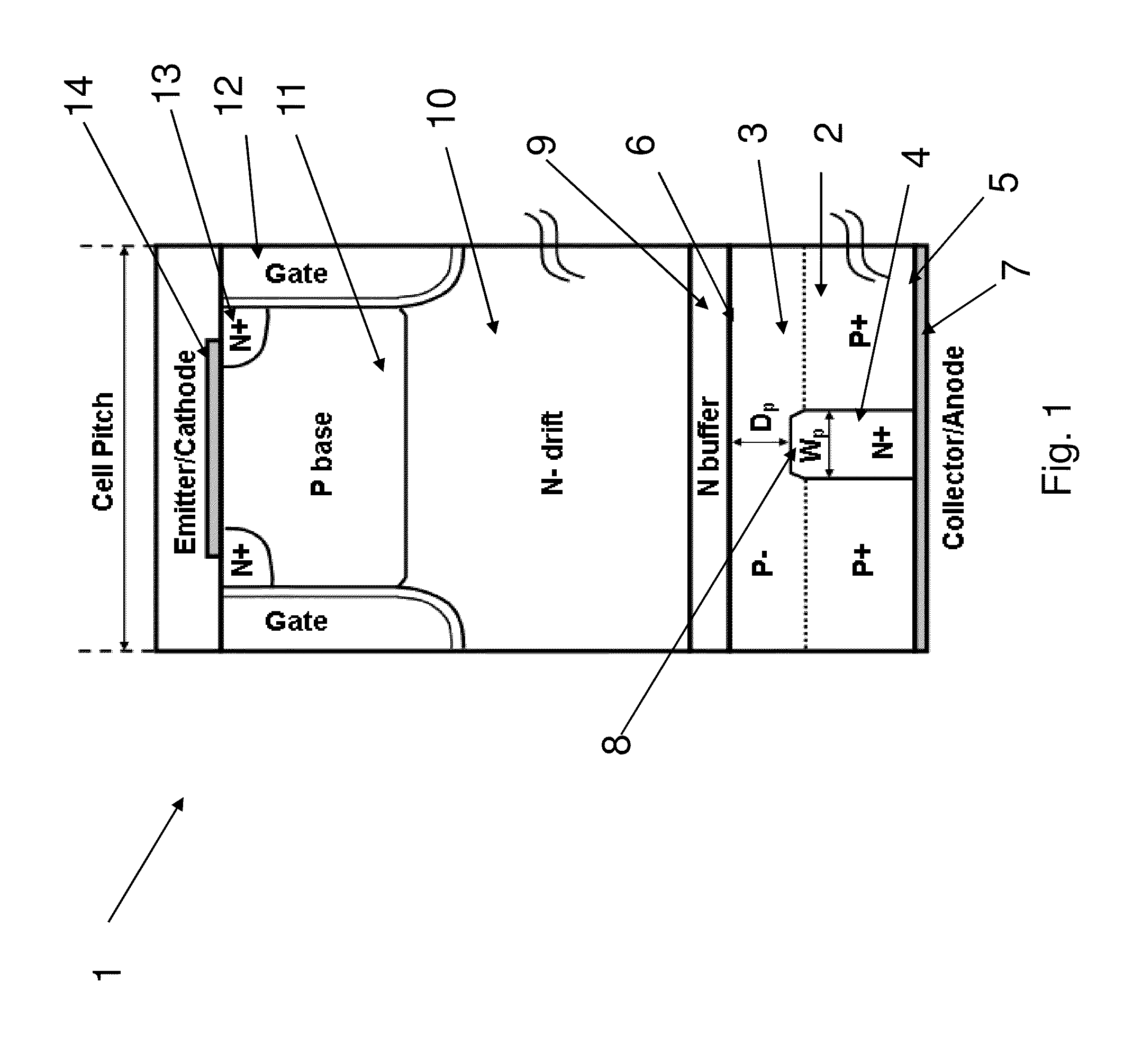
[0040]FIG. 1 is a schematic representation of a RC-IGBT structure according to the present invention. The transistor 1 is formed on a P-type substrate 2 which has a first surface 5 and a second surface 6 opposite to the first surface 5. A N+ column region 4 is formed on the first surface 5 which is along an anode / collector electrode 7. In addition, the P-type substrate is divided into two layers: the bottom layer is a highly-doped P+ layer 2, and the top layer is a lowly-doped P− layer 3. The interface between the P− layer 3 and the P+ layer 2 has a height which is about the same as the height of the N+ column region 4. There is provided a N-buffer region 9 above the P− layer 3, which is only present in a punch-through (PT) IGBT or a soft-punch-through IGBT. A N-drift region 10 is formed on the N-buffer region 9. There is also provided a P-base region 11 on the N-drift region 10 and a N+ region 13 on the P-base region 11. A gate region 12 is disposed to form a channel between the N+...


PUM


Abstract

An insulated gate bipolar transistor (IGBT) is provided comprising a semiconductor substrate having the following regions in sequence: (i) a first region of a first conductive type having opposing surfaces, a column region of a second conductive type within the first region extending from a first of said opposing surfaces; (ii) a drift region of the second conductive type; (iii) a second region of the first conductive type, and (iv) a third region of the second conductive type. There is provided a gate electrode disposed to form a channel between the third region and the drift region, a first electrode operatively connected to the second region and the third region, a second electrode operatively connected to the first region and the column region. The arrangement of the IGBT is such that the column region is spaced from a second surface of the opposing surfaces of the first region, whereby a forward conduction path extends sequentially through the third region, the second region, the drift region, and the first region, and whereby a reverse conduction path extends sequentially through the second region, the drift region, the first region and the column region. Reverse conduction of the IGBT occurs through a thyristor structure which is embedded in the IGBT. Such an IGBT structure is advantageous over a reverse conducting IGBT structure in which an anti-parallel diode is integrated or embedded because it provides improved reverse conduction and snapback performance.

Description

FIELD OF INVENTION[0001]The present invention relates to a reverse conducting bipolar transistor, and particularly to a reverse conducting insulated gate bipolar transistor (RC-IGBT) for use in power electronics applications.BACKGROUND TO THE INVENTION[0002]As a uni-directional conducting device, the insulated gate bipolar transistor (IGBT) requires an anti-parallel diode to release the energy stored in the inductive load in a transient turn-off state. Conventionally the anti-parallel diode is externally co-packed with the IGBT. This results in additional BOM (Bill of Material), additional testing time, and increased cost for the separate devices, and associated cost for the package. Moreover the approach of co-packing the IGBT and diode in one package increases the probable yield loss of the module, as failure of any of these devices results in malfunction of the whole part.[0003]Recently the development of reverse-conducting IGBTs (RC-IGBTs), i.e. the combination of the IGBT and t...

Claims


Application Information

Patent Timeline
Patent Type & Authority Applications(United States)
IPC IPC(8): H01L29/74H01L21/332
CPCH01L29/0834H01L29/7397H01L29/66348
Inventor UDREA, FLORINHSU, CHIH-WEILIN, WEI-CHIEH
Owner SINOPOWER SEMICON
Why Eureka
Try Eureka