Photoelectric conversion device and manufacturing method thereof

a technology of photoelectric conversion device and manufacturing method, which is applied in the direction of sustainable manufacturing/processing, final product manufacturing, vacuum evaporation coating, etc., can solve the problems of high manufacturing cost, difficult to make a photoelectric conversion device including the converter circuit thinner, and the photoelectric conversion device including the converter circuit cannot be manufactured. cost, the effect of reducing the cost of manufacturing the converter circuit and the conversion devi

Active Publication Date: 2011-10-27
SEMICON ENERGY LAB CO LTD
View PDF7 Cites 14 Cited by
  • Summary
  • Abstract
  • Description
  • Claims
  • Application Information

AI Technical Summary

Benefits of technology

[0035]According to an embodiment of the disclosed invention, a converter circuit is formed with the use of a thin film circuit including an oxide semiconductor film over a transmissive substrate, so that a photoelectric conversion device can be thinner.
[0036]Further, according to an embodiment of the disclosed invention, a converter circuit is formed with the use of a thin film circuit including an oxide semiconductor film, so that cost for manufacturing the converter circuit and a photoelectric conversion device including the converter circuit can be suppressed.
[0037]Further, according to an embodiment of the disclosed invention, a power device such as a converter circuit is formed using an oxide semiconductor film with wide band gap, so that temperature characteristics become stable. Therefore, the temperature characteristics of a photoelectric conversion device including the converter circuit can be stable.

Problems solved by technology

A solar cell needs no energy conversion from received light into thermal energy or kinetic energy in generating power, which is different from a conventional power generation method.
However, the converter circuit is formed using, for example, a power MOS, IGBT, a Schottky-barrier diode, or the like, so that manufacturing cost is high.
Further, it is unfortunately possible that the photoelectric conversion device including the converter circuit cannot be thinner because the converter circuit is thick (see Patent Document 2).
Accordingly, it is difficult to make a photoelectric conversion device including the converter circuit thinner.

Method used


Image

  • Photoelectric conversion device and manufacturing method thereof
  • Photoelectric conversion device and manufacturing method thereof
  • Photoelectric conversion device and manufacturing method thereof

Examples


embodiment 1

[0048]In this embodiment, photoelectric conversion devices each including a photoelectric conversion element and a converter circuit will be described with reference to FIGS. 1A and 1B, FIGS. 2A and 2B, FIGS. 3A to 3C, FIGS. 4A and 4B, FIGS. 5A and 5B, FIGS. 6A to 6E, and FIGS. 7A to 7C.

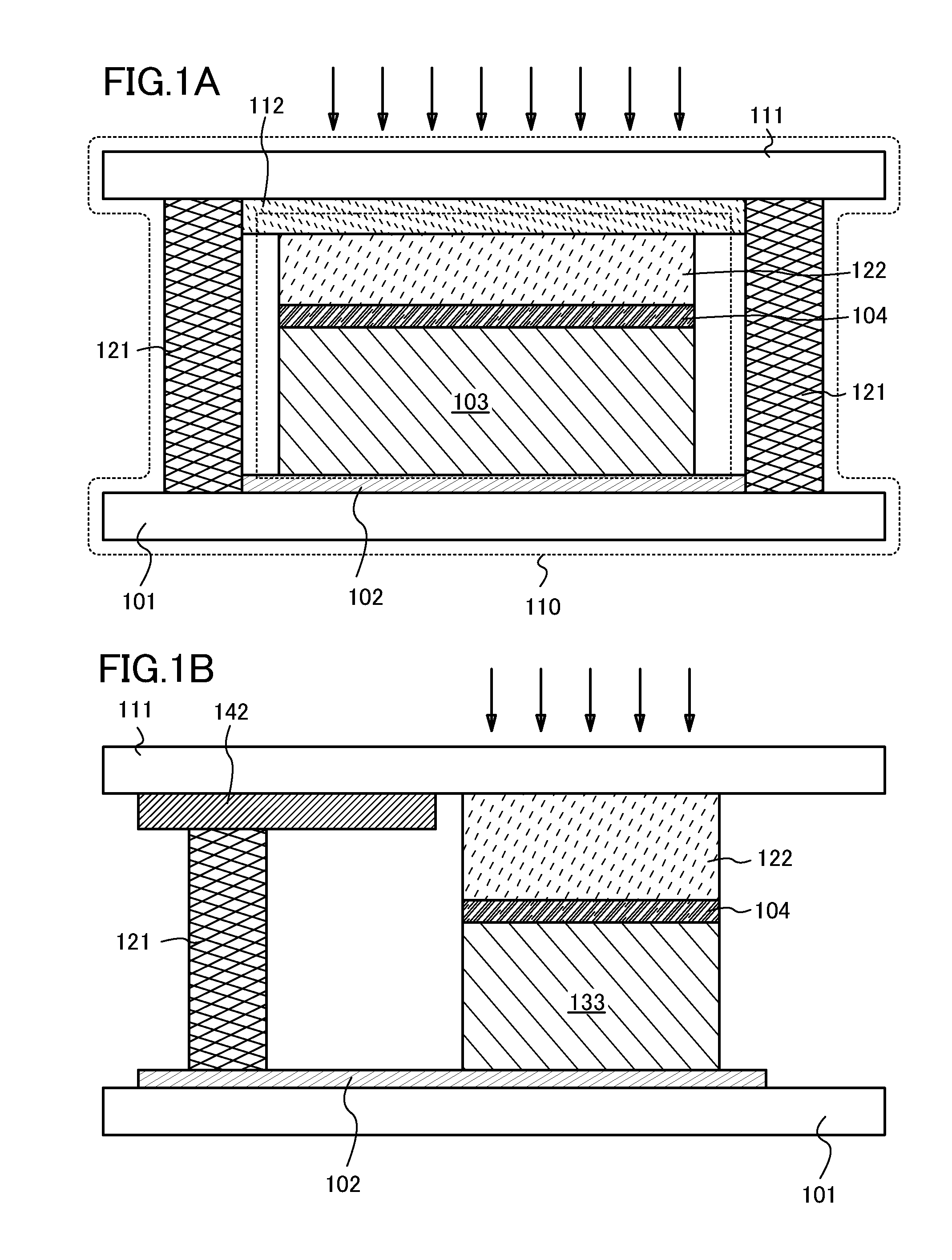
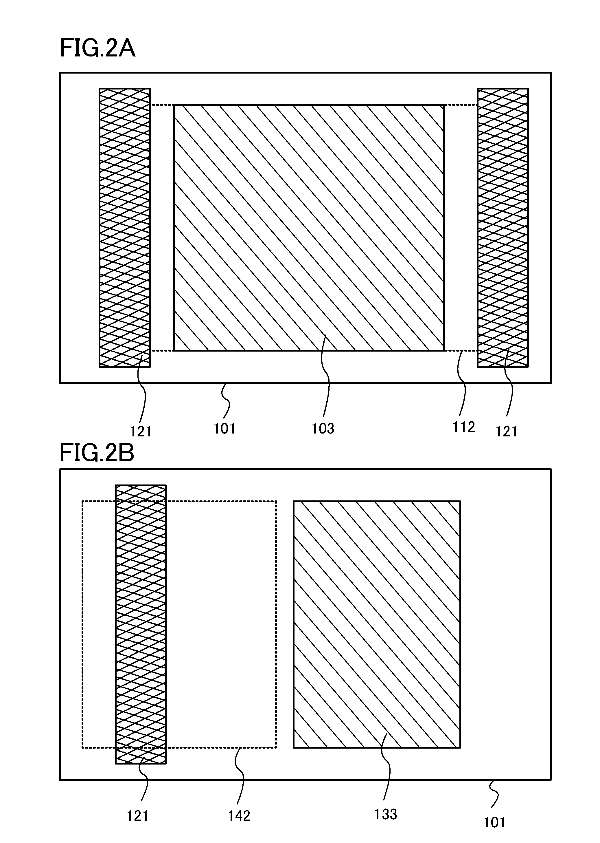
[0049]FIG. 1A and FIG. 2A illustrate the photoelectric conversion device of this embodiment. For comparison, FIG. 1B and FIG. 2B illustrate a conventional photoelectric conversion device.

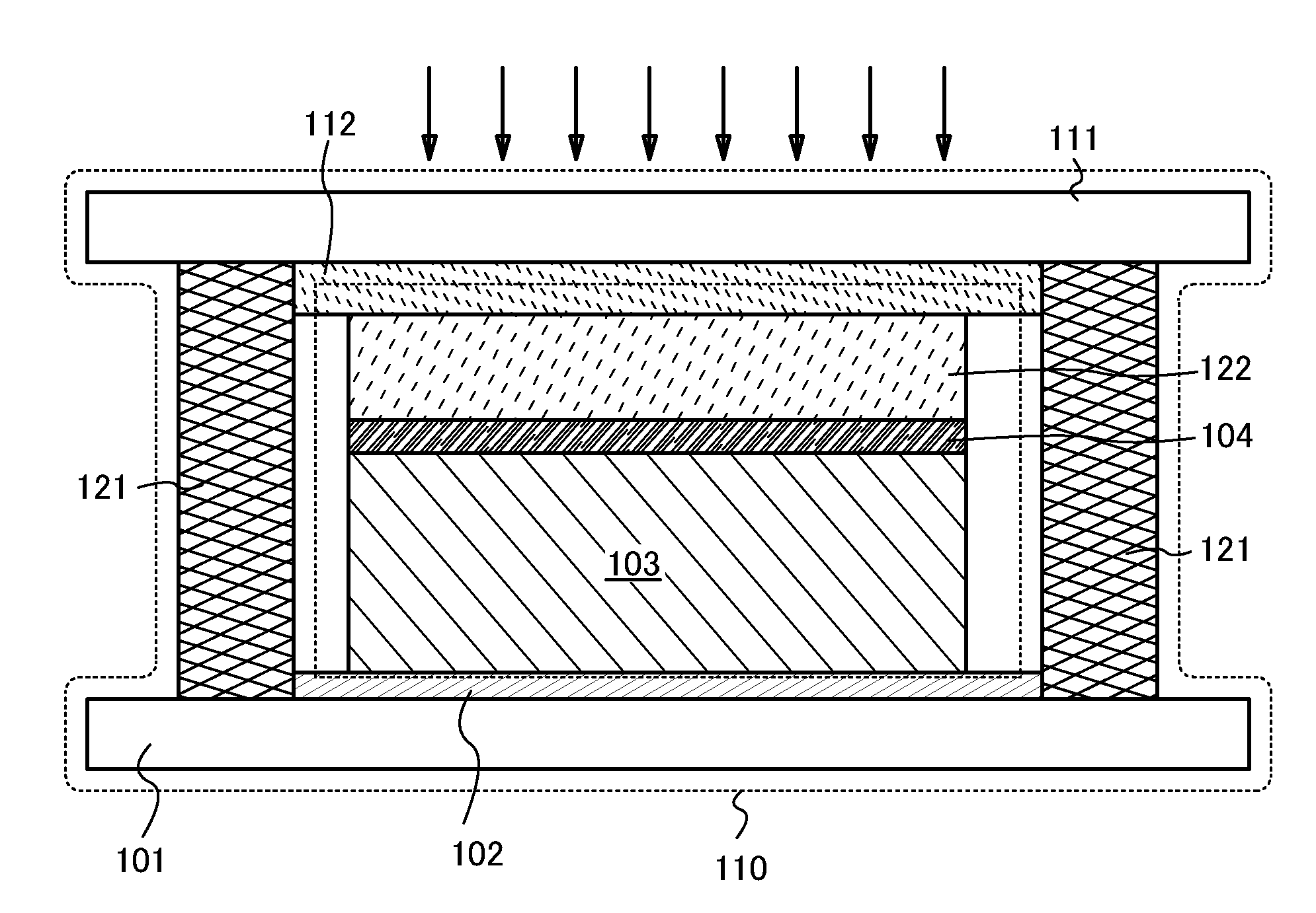
[0050]FIG. 1A illustrates a cross-sectional view of the photoelectric conversion device described in this embodiment.

[0051]The photoelectric conversion device illustrated in FIG. 1A includes, over a transmissive substrate 101, a transmissive conductive film 102, a photoelectric conversion element 103 provided in contact with the transmissive conductive film, a transmissive conductive film 104 provided in contact with the photoelectric conversion element 103. Further, the photoelectric conversion device illustrated in...

embodiment 2

[0247]In this embodiment, an example of a circuit structure of the converter circuit described in Embodiment 1 will be described with reference to FIG. 8.

[0248]FIG. 8 illustrates a structure example of a power source circuit 601. The power source circuit 601 includes a voltage conversion circuit 602 which is a converter circuit, and a control circuit 603 of the voltage conversion circuit 602. The voltage conversion circuit 602 is the DC-DC converter in Embodiment 1.

[0249]The voltage conversion circuit 602 includes a transistor 611, a coil 612, a diode 613, and a capacitor 614. The control circuit 603 includes a triangle wave generator circuit 621, a digital control circuit 650, a pulse width modulation output driver 623, a resistor 624, and a resistor 625. In addition, a dotted arrow 627 indicates a loop of a feedback circuit. A feedback voltage Vfb, which is an output voltage of the resistor 624, is input to the digital control circuit 650.

[0250]The transistor 410, the transistor 4...

embodiment 3

[0267]A solar photovoltaic module can be obtained by using the photoelectric conversion device obtained by any of Embodiment 1, 2, or the like. Described is an example in which the obtained solar photovoltaic module is mounted on a vehicle.

[0268]FIG. 9C illustrates an example of the solar photovoltaic module of this embodiment. The solar photovoltaic module of this embodiment is manufactured with the use of the photoelectric conversion device illustrated in Embodiment 1 or Embodiment 2.

[0269]A solar photovoltaic module 5028 in FIG. 9C includes, over the transmissive substrate 101, the transmissive conductive film 102; the photoelectric conversion element 103 provided in contact with the transmissive conductive film 102; and the transmissive conductive film 104 provided in contact with the photoelectric conversion element 103. Further, the solar photovoltaic module 5028 in FIG. 9C includes the converter circuit 112 formed using transmissive materials adjacent to the transmissive subs...


PUM

PropertyMeasurementUnit
thicknessaaaaaaaaaa
sheet resistanceaaaaaaaaaa
thicknessaaaaaaaaaa

Abstract

It is an object to reduce the region of a photoelectric conversion element which light does not reach, to suppress deterioration of power generation efficiency, and to suppress manufacturing cost of a voltage conversion element. The present invention relates to a transmissive photoelectric conversion device which includes a photoelectric conversion element including an n-type semiconductor layer, an intrinsic semiconductor layer, and a p-type semiconductor layer; a voltage conversion element which is overlapped with the photoelectric conversion element and which includes an oxide semiconductor film for a channel formation region; and a conductive element which electrically connects the photoelectric conversion element and the voltage conversion element. The photoelectric conversion element is a solar cell. The voltage conversion element includes a transistor having a channel formation region including an oxide semiconductor film. The voltage conversion element is a DC-DC converter.

Description

BACKGROUND OF THE INVENTION[0001]1. Field of the Invention[0002]One embodiment of the disclosed invention relates to a photoelectric conversion device and a manufacturing method thereof.[0003]2. Description of the Related Art[0004]As one of photoelectric conversion elements which directly convert received light into power by a photovoltaic effect to output the power, a solar cell can be given (see Patent Document 1). A solar cell needs no energy conversion from received light into thermal energy or kinetic energy in generating power, which is different from a conventional power generation method.[0005]Further, a photoelectric conversion device which has a solar cell and a converter circuit, which converts direct-current (DC) power generated by the solar cell, provided on a non-light receiving surface of the solar cell or the like has attracted attention as a small or middle-sized solar photovoltaic system or an emergency electric supply unit (see Patent Document 2 and Patent Documen...

Claims


Application Information

Patent Timeline
Patent Type & Authority Applications(United States)
IPC IPC(8): H01L31/0203
CPCC23C14/08H02S40/32H01L21/02422H01L21/02538H01L21/02554H01L21/02565H01L21/0262H01L21/02672H01L31/0296H01L31/0304H01L31/0312H01L31/03685H01L31/03762H01L31/0392H01L31/075H01L31/1816H01L31/202Y02E10/544Y02E10/548Y02E10/545C23C14/34Y02P70/50
Inventor YAMAZAKI, SHUNPEIKIMURA, HAJIMEITO, YOSHIAKIOHMARU, TAKURO
Owner SEMICON ENERGY LAB CO LTD
Why Eureka
Try Eureka