
Organic resistive random access memory and preparation method thereof

A resistive variable memory, an organic technology, applied in semiconductor/solid-state device manufacturing, semiconductor devices, electric solid-state devices, etc., can solve the obstacles to the practical application of organic resistive variable memory, poor chemical stability and thermal stability, and the difference between turn-on and turn-off voltages and other issues, to achieve low-cost electronic device applications, uniform trap distribution, and reduce instability

Active Publication Date: 2010-09-08
SEMICONDUCTOR MANUFACTURING INTERNATIONAL (BEIJING) CORP +1
View PDF4 Cites 6 Cited by
  • Summary
  • Abstract
  • Description
  • Claims
  • Application Information

AI Technical Summary

Problems solved by technology

Most of the organic materials selected for organic RRAM reported so far show poor chemical and thermal stability.
In addition, there are also problems with the stability of the resistance state transition of the device. For example, the conditions that lead to the transition state of the resistive material (such as the amplitude and time of the voltage pulse applied to the organic memory) will vary due to the fluctuation of different devices, and even For the same device, the turn-on and turn-off voltages required by the resistance switch and the values ​​of high resistance and low resistance generated will be different to a certain extent.
This large discreteness will make the device difficult to control precisely, which has become one of the main problems hindering the practical application of organic resistive memory.

Method used

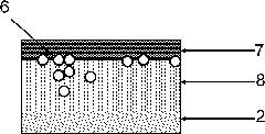
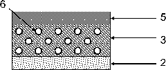

Image

  • Organic resistive random access memory and preparation method thereof
  • Organic resistive random access memory and preparation method thereof
  • Organic resistive random access memory and preparation method thereof

Examples


Embodiment Construction

[0028] The present invention will be further described below in conjunction with an embodiment, but the application of the present invention is not limited to the following specific examples of implementation.

[0029] In the present invention, the process flow for preparing the multi-state organic resistive variable memory is as follows:

[0030] 1) On the glass substrate, the vacuum degree is 4.5×10 -4 Pa, a layer of W was evaporated as the bottom electrode.

[0031] 2) Before the organic titanyl phthalocyanine film is grown by thermal evaporation, the metal Al, Hf or Mg powder and the organic titanyl phthalocyanine powder are ground and stirred evenly, and the mass percentage of the metal is 0.1% to 1%. Then use the mask plate at a vacuum of 4.5×10 -4 Under Pa, a metal-doped titanyl phthalocyanine thin film (with a thickness of 100-200 nm) is evaporated at a temperature of 200°C-250°C, and a lead-out hole for the bottom electrode is formed.

[0032] 3) Place the mask pla...


PUM


Abstract

The invention provides an organic resistive random access memory and a preparation method thereof, which belong to the technical field of very large scale integrated circuit. The organic resistive random access memory comprises a substrate, a bottom electrode on the substrate, a middle organic functional layer and a top electrode, wherein the middle organic functional layer is a metal-doped TiOPc film. During the growth process of the TiOPc film, the even metal doping is introduced to realize the redox reaction of the metal impurity and the organic thin film and to further realize the resistive bistable state. Meanwhile, the even metal doping is artificially introduced to realize the even trap distribution, thereby effectively reducing the instability of the characteristics of a single device and the inhomogeneity of resistive characteristics among different devices, caused by the trap random distribution. The organic resistive random access memory has good chemical stability and temperature stability, and can be realized on the soft substrate, and has high application value in the field of the organic memory with low cost and high performance.

Description

technical field [0001] The invention belongs to the technical field of ultra-large-scale integrated circuits, and in particular relates to an organic resistive variable memory and a preparation method thereof. Background technique [0002] In today's digital age of information explosion, people's production and life cannot do without high-density, high-speed memory. At present, the most widely used and most developed non-volatile memory is a flash memory (flash memory) device. With the advancement of microelectronic technology nodes, flash memory based on the traditional floating gate structure is approaching its physical limit, seriously affecting the storage function of the unit, and unable to follow the footsteps of Moore's Law for integrated circuits. A new generation of resistive memory (RRAM) with higher storage density, faster response speed, lower operating voltage, and simpler manufacturing process has emerged. Because of its potential to replace flash memory, it h...

Claims


Application Information

Patent Timeline
Patent Type & Authority Applications(China)
IPC IPC(8): H01L51/05H01L51/40
Inventor 于哲黄如邝永变张丽杰高德金
Owner SEMICONDUCTOR MANUFACTURING INTERNATIONAL (BEIJING) CORP
Learn More