Non-volatile resistance-switching thin film devices

a thin film, non-volatile technology, applied in the direction of discharge tube main electrodes, conductors, instruments, etc., can solve the problems of poor cycle fatigue performance, device general power consumption, and strong influence of switching cycle number, and achieve the effect of not losing switching time or stability

Active Publication Date: 2011-11-03
THE TRUSTEES OF THE UNIV OF PENNSYLVANIA
View PDF2 Cites 11 Cited by
  • Summary
  • Abstract
  • Description
  • Claims
  • Application Information

AI Technical Summary

Benefits of technology

[0021]The device above may be non-volatile and thus does not require the continuous application of either voltage or current to maintain resistance states. It is also desirable that the device be capable of switching between a low and high resistance state repeatedly without a loss of switching time or stability.

Problems solved by technology

However, the number of switching cycles performed strongly affects set voltage.
Thus, these devices generally exhibit high power consumption and poor cycle fatigue performance.
These materials, however, tend to suffer from cycle fatigue and retention problems.
Moreover, many magnetoresistive oxide devices require magnetic switching fields and require low operating temperatures.
Early efforts with perovskite materials required relatively high voltages and the EPIR effect tends to be cycle dependant.
However, the devices made from perovskite materials are largely incompatible with the semiconductor industry due to their crystal structures and the difficulties in manufacturing these materials on silicon substrates.
These metal oxide devices, however, suffer from incompatibility with silicon based semiconductor industry, and may also suffer from a lack of scalability.
Further, many of the aforementioned techniques and devices have not shown scalability for future devices, such as those expected to be in the 22 nm range for the year 2016.

Method used


Image

  • Non-volatile resistance-switching thin film devices
  • Non-volatile resistance-switching thin film devices
  • Non-volatile resistance-switching thin film devices

Examples


examples

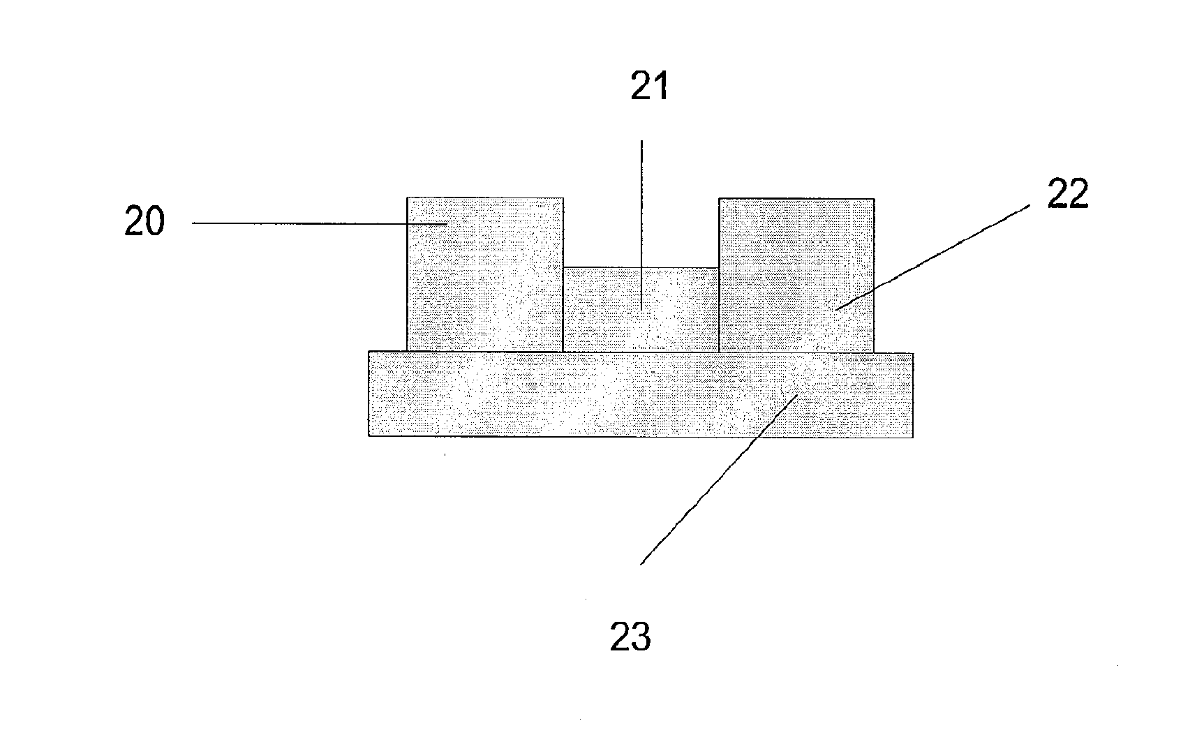
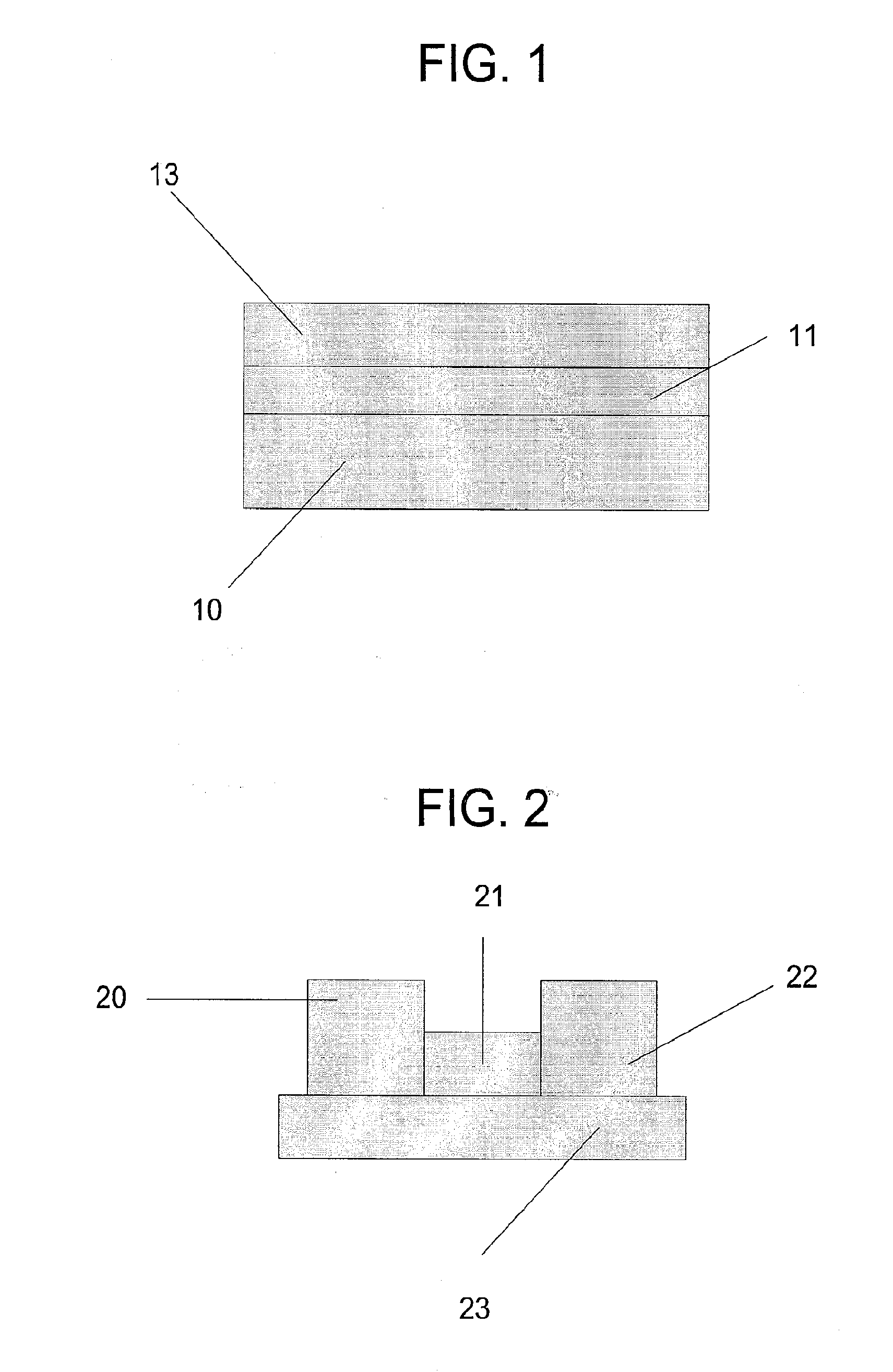
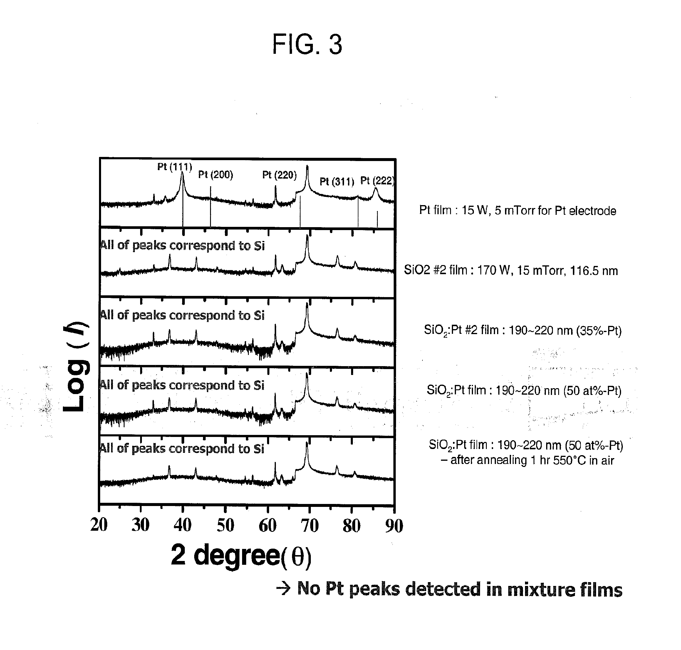
[0064]An example of a resistance-switching memory device is described using single crystal silicon n-type or p-type silicon with 100 or 110 orientations as the substrate, SrRuO3 as the bottom electrode, Pt as the top electrode, and SiO2 / Pt as the amorphous mixture layer. The various materials above do not share a common structure, and indeed the mixture layer can be deposited on unheated substrates. The test cells in the current example device had a diameter of 80 microns (“μm”).

[0065]The bottom electrode was deposited by pulse laser deposition using a KrF laser with laser energy of 200 mJ at a repetition frequency of 1-15 Hz in an O2 pressure of 0.01-100 mTorr. The film thickness, orientation and crystallinity were determined by a theta-2 theta diffractometer and a four circle x-ray diffractometer, both using a Cu Kα source. The surface morphology was observed by atomic force microscopy.

[0066]Because the silicon substrate may be covered by a layer of native oxide of an amorphous na...


PUM

PropertyMeasurementUnit
distanceaaaaaaaaaa
distanceaaaaaaaaaa
distanceaaaaaaaaaa

Abstract

Disclosed herein is a resistive switching device having an amorphous layer comprised of an insulating silicon-containing material and a conducting material. The amorphous layer may be disposed between two or more electrodes and be capable of switching between at least two resistance states. Circuits and memory devices including resistive switching devices are also disclosed, and a composition of matter involving an insulating silicon-containing material and a conducting material comprising between 5 and 40 percent by molar percentage of the composition is disclosed herein as well. Also disclosed herein are methods for switching the resistance of an amorphous material.

Description

CROSS-REFERENCE TO RELATED APPLICATION[0001]This patent application is a PCT International application claiming priority to U.S. Provisional Application 61 / 139,028 filed Dec. 19, 2008, the entirety of which is incorporated by reference herein.STATEMENT OF GOVERNMENT INTERESTS[0002]At least a portion of the work leading to the disclosed inventions was made using federal support by the National Science Foundation under grants number DMR07-05054 and DMR-05-20020. Accordingly, the U.S. government may have rights to the disclosed inventions.TECHNICAL FIELD[0003]The disclosed inventions generally relate to semiconductor devices, and more particularly to resistance-switching semiconductor devices. The disclosed inventions also generally relate to resistance-switching material compositions.BACKGROUND[0004]Resistance-switching behavior is well known in the art and has been observed and studied in some metal-insulator mixtures since the mid 1970's. Reversible resistance-switching devices are ...

Claims


Application Information

Patent Timeline
Patent Type & Authority Applications(United States)
IPC IPC(8): H01L45/00H01B1/02H01L21/62
CPCG11C13/0002G11C13/0009G11C2213/33H01L45/14H01L45/1226H01L45/1233H01L45/10H10N70/25H10N70/823H10N70/881H10N70/826
Inventor CHEN, I-WEIKIM, SOO GILCHEN, ALBERTWANG, YUDI
Owner THE TRUSTEES OF THE UNIV OF PENNSYLVANIA
Why Eureka
Try Eureka