Semiconductor device and method of manufacturing the device

a semiconductor and semiconductor technology, applied in the direction of semiconductor devices, basic electric elements, electrical equipment, etc., can solve the problems of increasing on-resistance and increasing on-resistance, and achieve the effect of reducing on-resistan

Active Publication Date: 2011-11-03
PANASONIC CORP
View PDF4 Cites 24 Cited by
  • Summary
  • Abstract
  • Description
  • Claims
  • Application Information

AI Technical Summary

Benefits of technology

[0020]According to the semiconductor device and the method of manufacturing the device of the present disclosure, on-resistance can be reduced in a semiconductor device such as a junction field effect transistor.

Problems solved by technology

However, a conventional JFET has the problem that on-resistance increases when a threshold voltage is raised in a positive direction.
An increase in the on-resistance due to the current collapse is a crucial problem in a power transistor in which a high drain voltage is applied.

Method used


Image

  • Semiconductor device and method of manufacturing the device
  • Semiconductor device and method of manufacturing the device
  • Semiconductor device and method of manufacturing the device

Examples


Embodiment Construction

ction field effect transistor.

BRIEF DESCRIPTION OF THE DRAWINGS

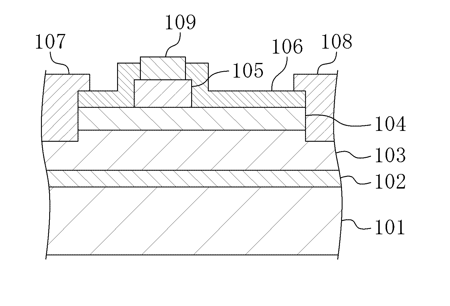
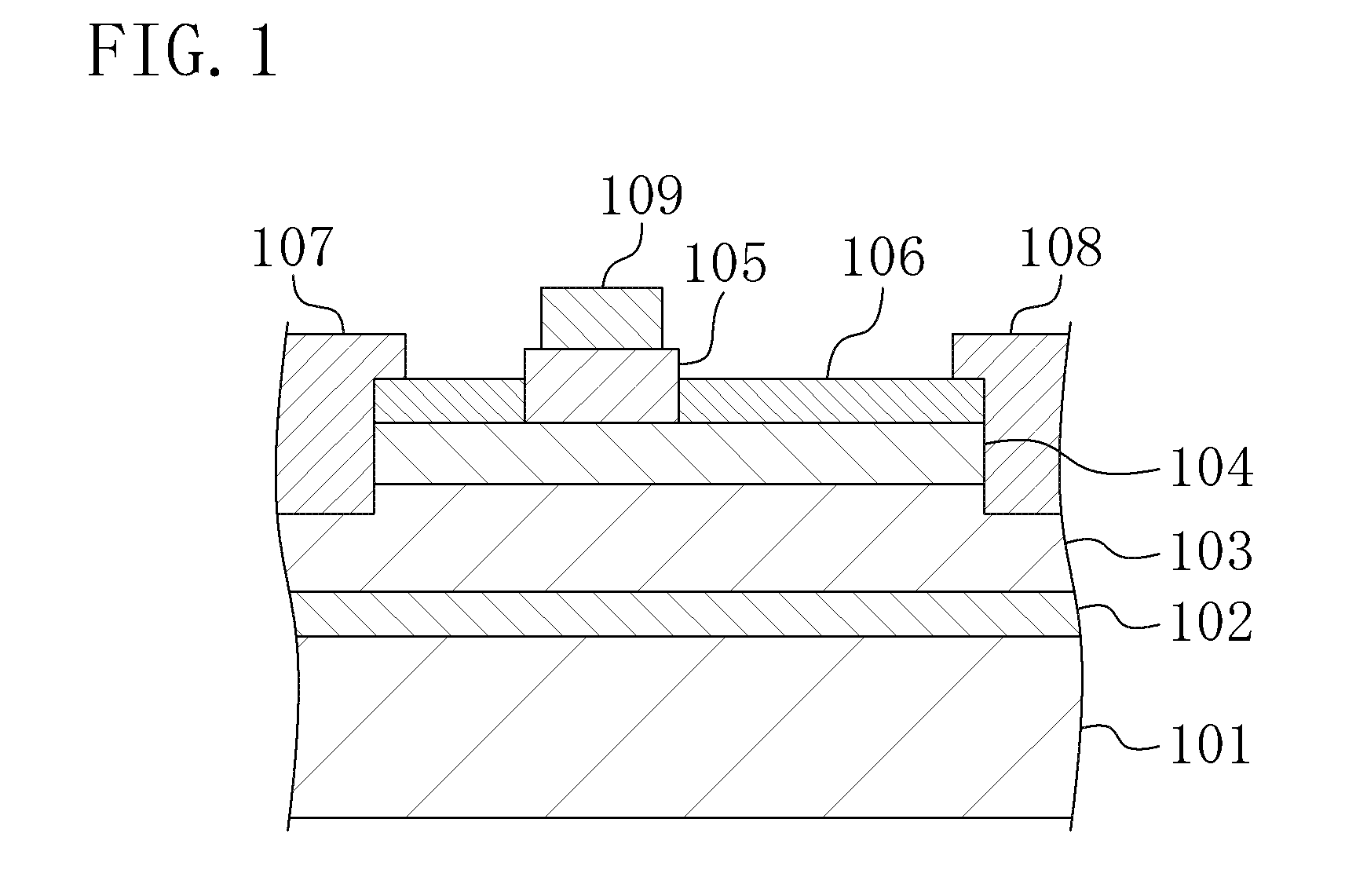
[0021]FIG. 1 is a cross-sectional view illustrating a semiconductor device according to an embodiment.

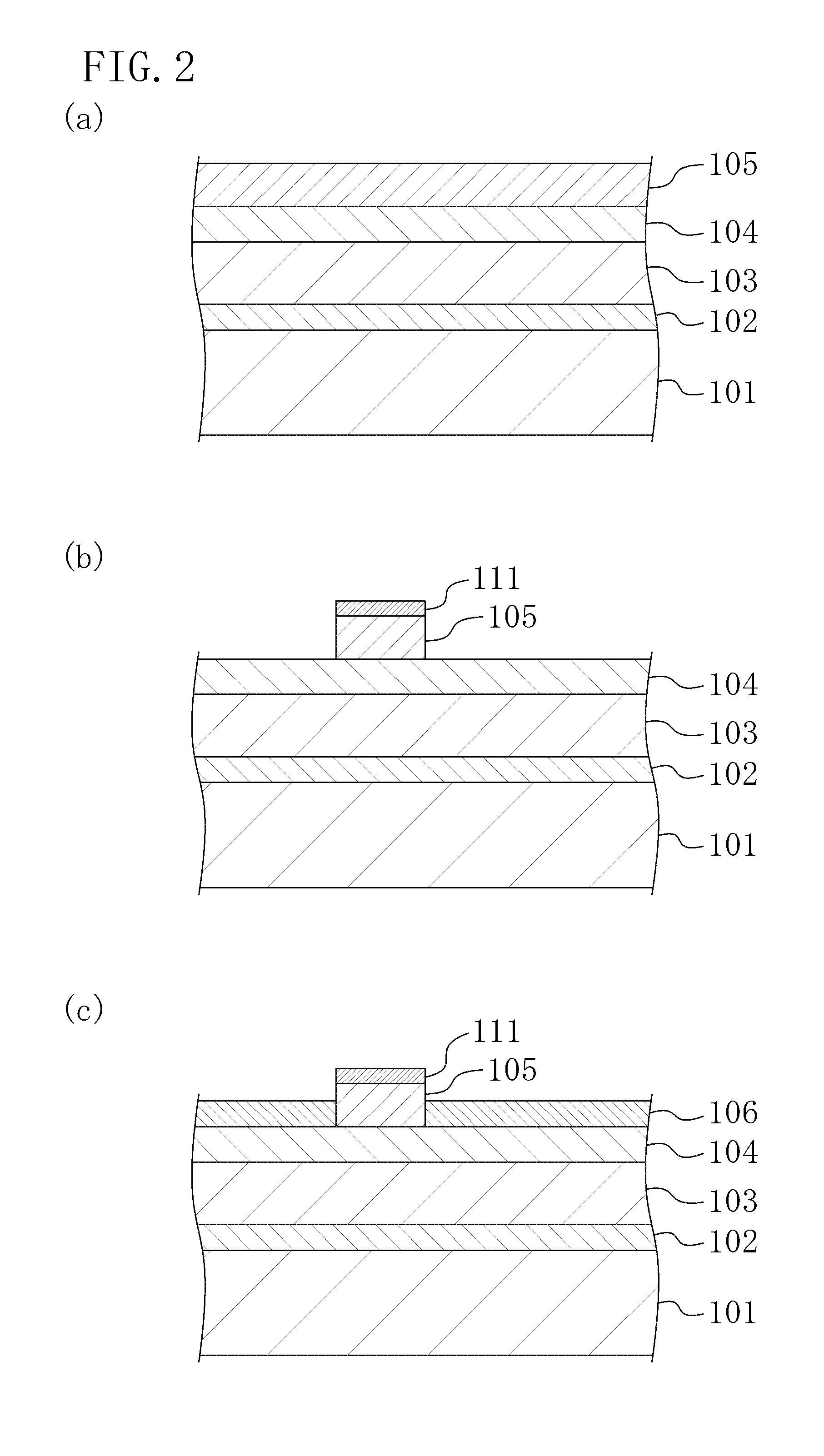
[0022]FIGS. 2A-2C are cross-sectional views illustrating a manufacturing method of a semiconductor device according to an embodiment in order of steps.

[0023]FIGS. 3A and 3B are cross-sectional views illustrating a manufacturing method of a semiconductor device according to an embodiment in order of steps.

[0024]FIGS. 4A and 4B are cross-sectional views illustrating a variation of the manufacturing method of the semiconductor device according to the embodiment in order of steps.

[0025]FIG. 5 is a cross-sectional view illustrating a variation of the semiconductor device according to the embodiment.

[0026]FIG. 6 is a cross-sectional view illustrating a variation of the semiconductor device according to the embodiment.

DETAILED DESCRIPTION

[0027]FIG. 1 illustrates a cross-sectional structure of a semiconductor device according to...


PUM


Abstract

In a manufacturing method of a semiconductor device, first, a first semiconductor layer, a second semiconductor layer, and a p-type third semiconductor layer are sequentially epitaxially grown on a substrate. After that, the third semiconductor layer is selectively removed. Then, a fourth semiconductor layer is epitaxially grown on the second semiconductor layer. Then, a gate electrode is formed on the third semiconductor layer.

Description

CROSS-REFERENCE TO RELATED APPLICATION[0001]This is a continuation of PCT International Application PCT / JP2009 / 006873 filed on Dec. 15, 2009, which claims priority to Japanese Patent Application No. 2009-070186 filed on Mar. 23, 2009. The disclosures of these applications including the specifications, the drawings, and the claims are hereby incorporated by reference in their entirety.BACKGROUND[0002]The present disclosure relates to semiconductor devices and methods of manufacturing the devices, and more particularly to power transistors using nitride semiconductor and methods of manufacturing the transistors.[0003]In recent years, field effect transistors (FETs) using gallium nitride (GaN) semiconductor have been actively researched as high-frequency high-power devices. GaN can form various alloys with aluminum nitride (AlN) and indium nitride (InN). Therefore, similar to conventional arsenic semiconductor such as gallium arsenide (GaAs) semiconductor, a heterojunction can be forme...

Claims


Application Information

Patent Timeline
Patent Type & Authority Applications(United States)
IPC IPC(8): H01L29/772H01L29/205H01L21/20
CPCH01L29/1066H01L29/7787H01L29/66462H01L29/2003
Inventor HIKITA, MASAHIROTANAKA, KENICHIROUEDA, TETSUZO
Owner PANASONIC CORP
Why Eureka
Try Eureka