Method of patterning thin film solution-deposited

a thin film and solution-deposited technology, applied in the direction of basic electric elements, electrical apparatus, semiconductor devices, etc., can solve the problems of low mobility, poor performance of solution-processed tfts, and long-term instability of organic semiconductors, etc., to achieve the effect of reducing the number of deposited solutions, reducing the difficulty of selectively deposited solution-state materials on substrates, and improving the stability of the substra

Inactive Publication Date: 2011-11-17
IND ACADEMIC CORP FOUND YONSEI UNIV
View PDF0 Cites 5 Cited by
  • Summary
  • Abstract
  • Description
  • Claims
  • Application Information

AI Technical Summary

Benefits of technology

[0016]Also provided is a method of patterning a thin film, in which a pattern desired by a user can be formed on a solution-processed thin film irrespective of limitations of a shadow mask, that is, without limitations as to size, such as limitations in the size (e.g., 25 μm) of openings formed in the mask.
[0017]Also provided is a method of pattering a solution-deposited thin film, in which a pattern having a complicated shape desired by a user can be formed through a simplified process.

Problems solved by technology

However, the organic semiconductors have fundamental limitations of low mobility, environment-sensitive performance, and unstable long term.
Since the solution-processed TFTs also exhibit poor performance compared to typical vacuum-processed TFTs, active research is currently underway, particularly in order to improve the mobility and lower the annealing temperature.
Meanwhile, the development of patterning processes is an issue that is no less important than the solution deposition process, because it is very difficult to selectively deposit a solution-state material on a substrate using a shadow mask, even though selective deposition using a shadow mask is possible in a typical vacuum deposition process.
Although conventional lithography can advantageously be used to realize high-resolution patterns, its expensive and complicated procedure overshadows the benefits of the solution process.
Although the ultimate goal of studying oxide semiconductors is to realize fully transparent all-oxide devices, the chemical etching associated with lithography may not provide sufficient selectivity among similar oxide materials.
However, the problems of low spatial resolution and poor edge resolution still remain as challenges to overcome.
Although this technique is intended to be used to pattern a thin film using a laser, it fails to replace photolithography because its resolution and process rate are limited.
Although conventional LIFT can be useful for forming a pattern of a simple material that can be easily evaporated or melted, it is not appropriate for a material having a complicated structure, or for cases in which the unique properties of a material must be maintained without phase transition.
Although this technique is advantageous in that the material that is intended to be transited does not evaporate or melt, it is disadvantageous in that an additional process, in which the absorption layer must be additionally formed between the substrate and a thin film, is required.
However, this technique has a limited ability to rapidly form patterns having various shapes and sizes, and it is difficult to control the cross-sectional shape of the pattern.
Otherwise, the interval between pulses increases, and a long time is spent for the entire patterning process.
However, printing requires minimum pulse energy.
However, patterning techniques that have been devised to date have problems in that they are time-consuming and incur high expenses attributable to complicated multistage processes if the shape and period of a pattern can be controlled, and in that the shape and period of a pattern cannot be freely controlled in the case of self-assembly, in which the process itself is relatively simple.
However, the techniques disclosed in the above-mentioned documents are limited in their applicability to the formation of complicated pattern shapes, since they involve serial processing, which fundamentally belongs to the category of the LIFT technique.
These techniques also fail to provide a specific solution to the application of a solution-deposited thin film to patterning.

Method used


Image

  • Method of patterning thin film solution-deposited
  • Method of patterning thin film solution-deposited
  • Method of patterning thin film solution-deposited

Examples


Embodiment Construction

[0034]Reference will now be made in detail to various embodiments of the present invention, examples of which are illustrated in the accompanying drawings and described below. While the invention will be described in conjunction with exemplary embodiments, it is to be understood that the present description is not intended to limit the invention to those exemplary embodiments. On the contrary, the invention is intended to cover not only the exemplary embodiments, but also various alternatives, modifications, equivalents and other embodiments that may be included within the spirit and scope of the invention as defined by the appended claims.

[0035]In the following description of the present invention, detailed descriptions of technical constitutions related to thin film patterning that are well known in the art will be omitted.

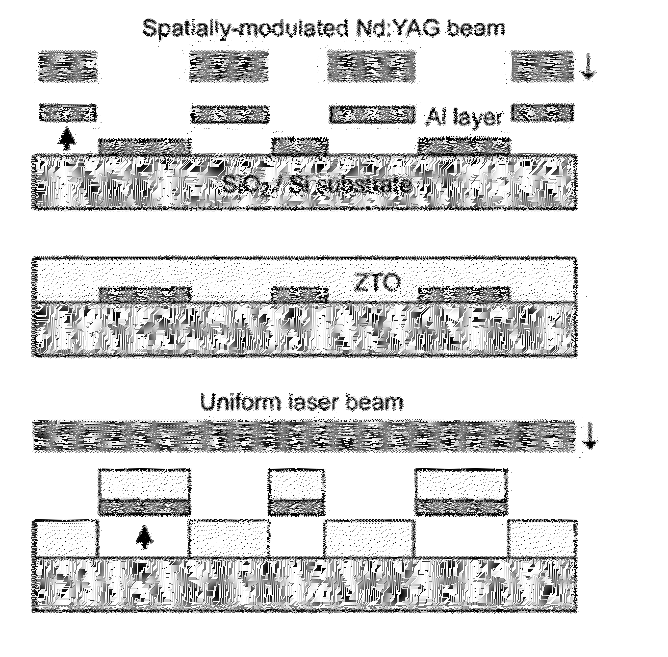
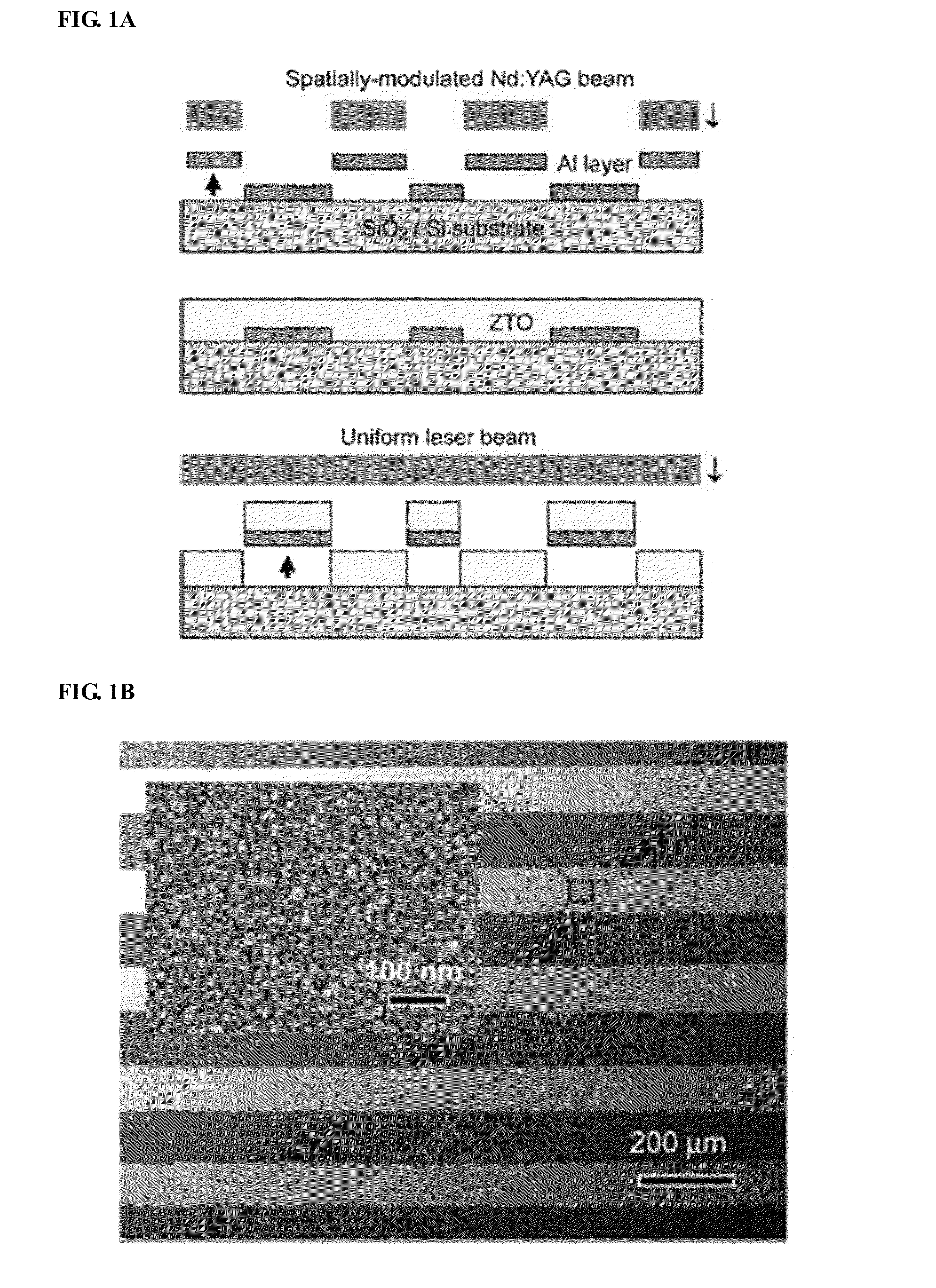
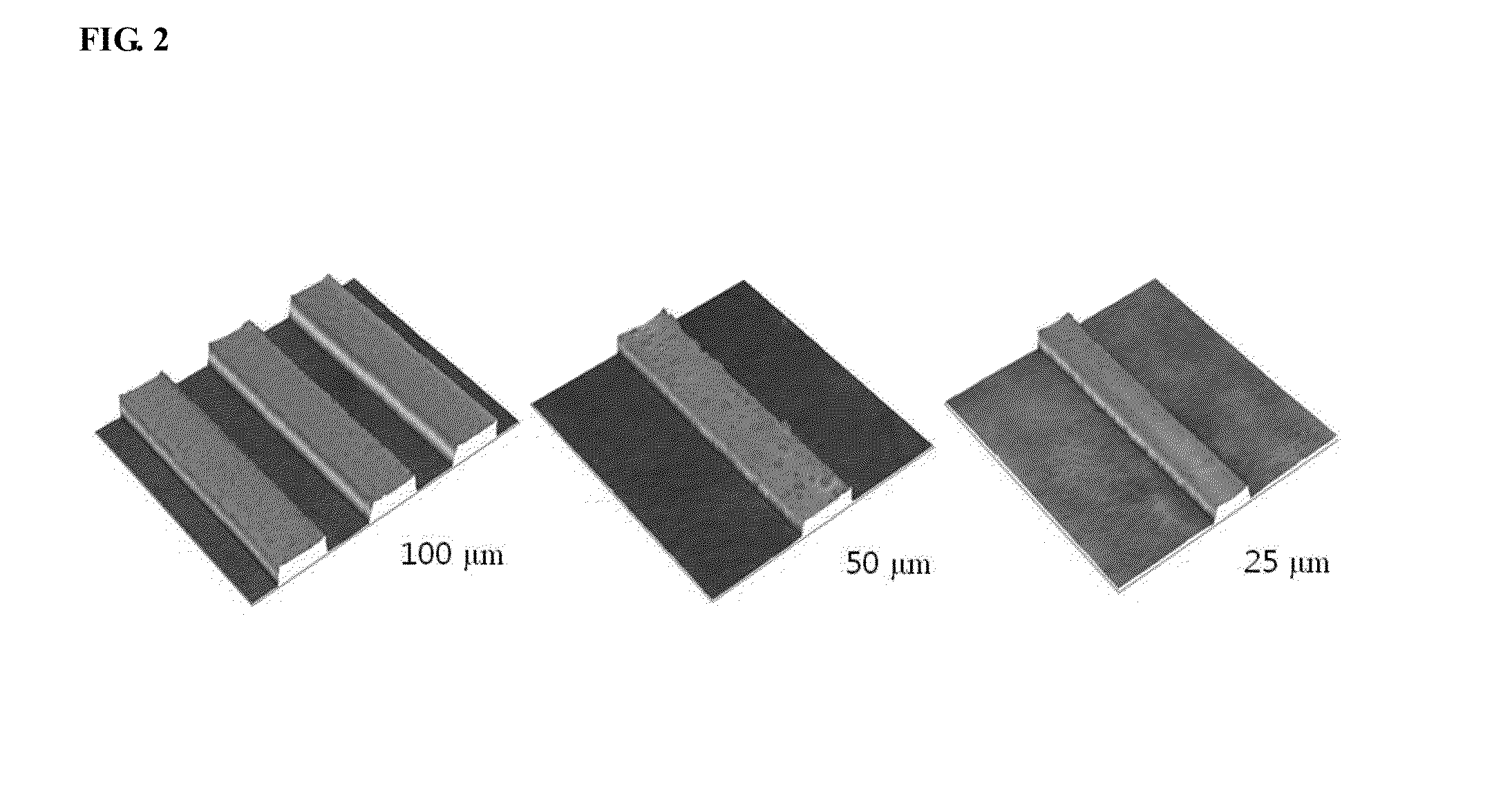
[0036]FIGS. 1A and 1B are views schematically showing a process of performing a method of patterning a thin film according to an exemplary embodiment of the pre...


PUM


Abstract

A method of patterning a solution-deposited thin film is provided. The method includes photoetching a pattern in a laser absorption metal layer by allowing a pulsed laser beam to pass through a spatial optical modulator so that the laser beam is radiated on the metal layer, the pattern corresponding to the spatial optical modulator; solution-depositing an oxide layer over a surface of the substrate that is exposed to an outside and a surface of the patterned metal layer; patterning the solution-deposited oxide layer by radiating a pulsed laser beam directly on the solution-deposited oxide layer without passing through the spatial optical modulator, and heating the metal layer underlying the oxide layer to induce thermo-elastic force, so that the metal layer is detached along with the overlying oxide layer from the substrate.

Description

CROSS REFERENCE TO RELATED APPLICATION[0001]The present application claims priority from Korean Patent Application Number 10-2010-0045884 filed on May 17, 2010, the entire contents of which application are incorporated herein for all purposes by this reference.BACKGROUND OF THE INVENTION[0002]1. Field of the Invention[0003]The present invention relates to a thin film patterning process, and more particularly, to a method that allows high-resolution patterning to be performed on a solution-deposited oxide semiconductor thin film without using either a photoresist or chemical etching.[0004]2. Description of Related Art[0005]Oxide semiconductors have drawn great interest for use in various optoelectronic applications, such as transparent electronics, Light-Emitting Diodes (LEDs) and photodetectors. The main benefit of oxide materials is that they enable low-temperature deposition, which is compatible with plastic substrates, and can provide higher mobilities than amorphous silicon (Si)...

Claims


Application Information

Patent Timeline
Patent Type & Authority Applications(United States)
IPC IPC(8): H01L29/12H01L21/20
CPCH01L21/02381H01L21/02488H01L21/02491H01L21/02494H01L29/7869H01L21/02565H01L21/02628H01L21/02658H01L21/02554
Inventor LEE, MYEONG KYU
Owner IND ACADEMIC CORP FOUND YONSEI UNIV
Why Eureka
Try Eureka