Methods for Casting By a Float Process and Associated Apparatuses

a float process and float technology, applied in the direction of sustainable manufacturing/processing, silicon compound, final product manufacturing, etc., can solve the problems of difficult process scaling up, energy and capital intensive solar cells from single and multi-crystalline ingots of high purity silicon, and the process of wafer making is still largely inefficient, etc., to achieve rapid scale-up, high rate, and high efficiency

Inactive Publication Date: 2011-11-17
CARNEGIE MELLON UNIV
View PDF7 Cites 11 Cited by
  • Summary
  • Abstract
  • Description
  • Claims
  • Application Information

AI Technical Summary

Benefits of technology

[0017]1. It uses cheap raw materials for molten slag preparation, inexpensive process equipment and allows for rapid scale-up from laboratory to pilot to industrial scale.
[0018]2. The process can be made continuous and can produce ribbons at a high rate since horizontal crystallization in the Si<111> configurational structure is obtained. Other crystalline structures can also be produced since the growth in the horizontal direction on a liquid substrate allows the crystal to form in the absence of nucleation sites.
[0020]4. The process can reduce the cost of wafering by a factor of at least 2-3 relative to the current wire saw process.
[0022]Other purposes of using a glassy layer include minimizing chemical interactions, preventing entrainment, and providing sufficient wettability and interfacial stability with respect to the working molten substrate layer during spreading followed by solidification and crystal growth.

Problems solved by technology

Semiconductor wafer have become a commodity in many cases, but the process of making wafers is still largely inefficient.
Making solar cells from single and multi-crystalline ingots of high purity Silicon is energy and capital intensive.
The process is difficult to scale up due to the batch nature of many of the processing steps and the wafer process is inefficient.
The wires used to cut the slabs into wafers are as thick as the wafers themselves and half of the material is therefore lost in the sawing process.
This cutting material is difficult to recycle since it is mixed with iron from the wire and cutting oil.
These issues make it difficult and inefficient to make very thin wafers.
These deficiencies are particularly problematic in the production of solar cells where production cost is one factor which limits widespread acceptance.
Due to the polycrystalline nature of the seed layer, heavily defective grains always remain present in the epitaxial layer.
As observed in the float glass process, defects arise when the voltatilized materials from the molten surface are advected and diffused in the gas flow followed by their dropping on the top surface glass.
These polysilicon films are limited by the non-uniformity and low electron mobility.

Method used


Image

  • Methods for Casting By a Float Process and Associated Apparatuses
  • Methods for Casting By a Float Process and Associated Apparatuses
  • Methods for Casting By a Float Process and Associated Apparatuses

Examples


Embodiment Construction

[0042]1. The Invention

[0043]1.1 The Invention Generally

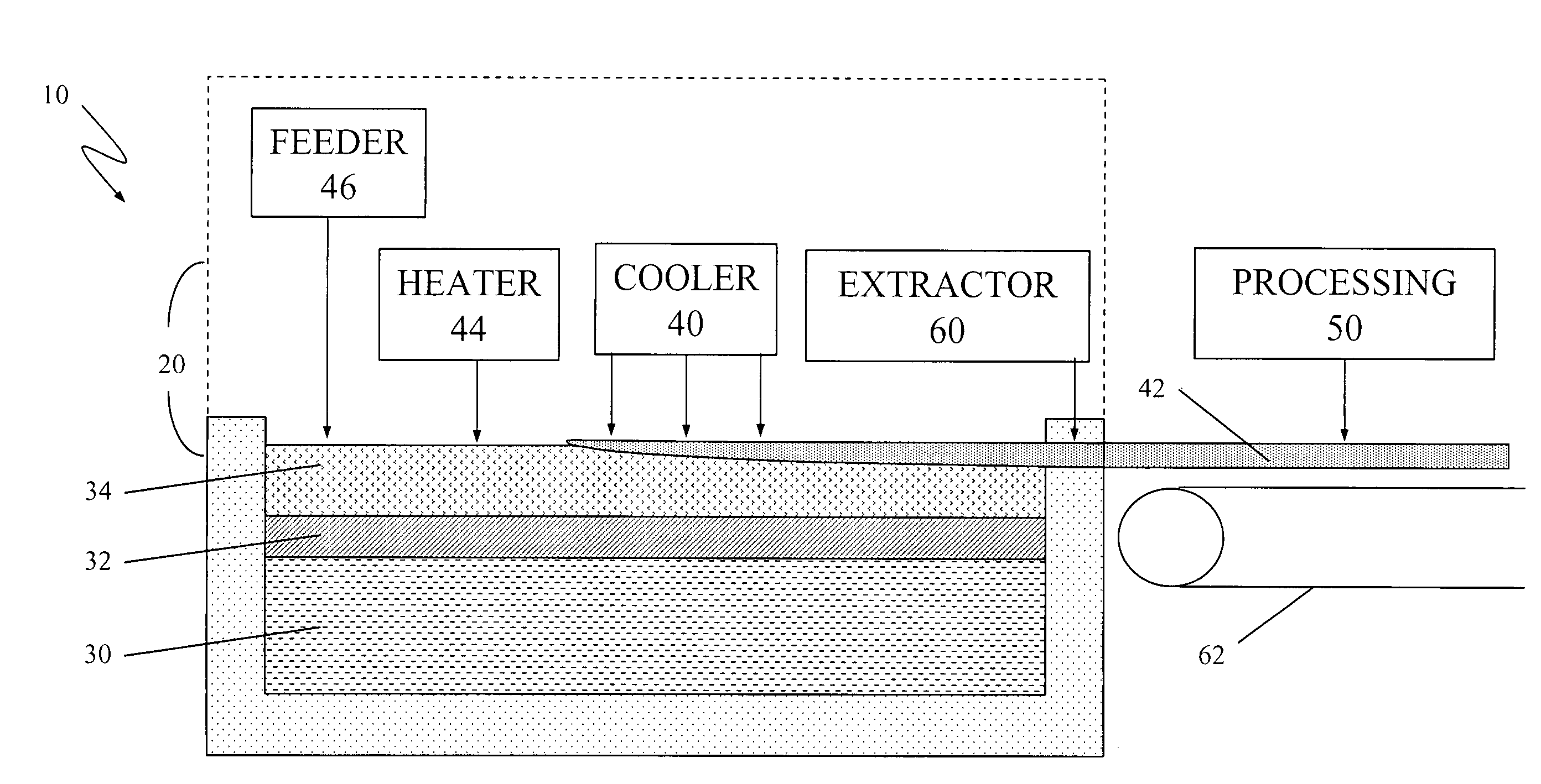
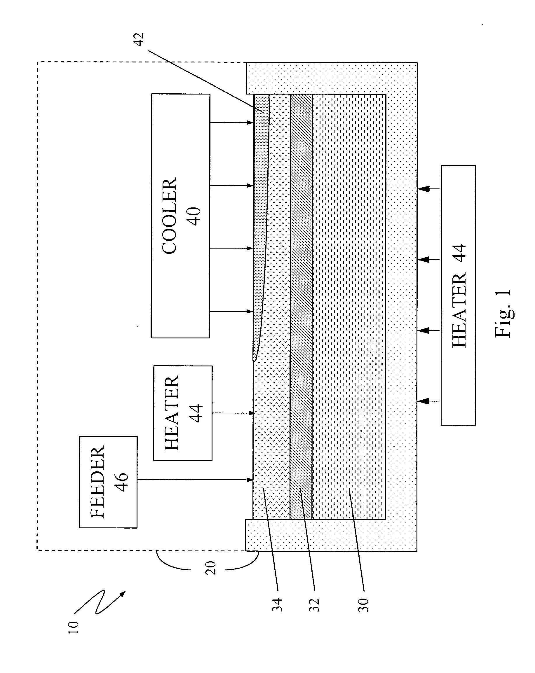
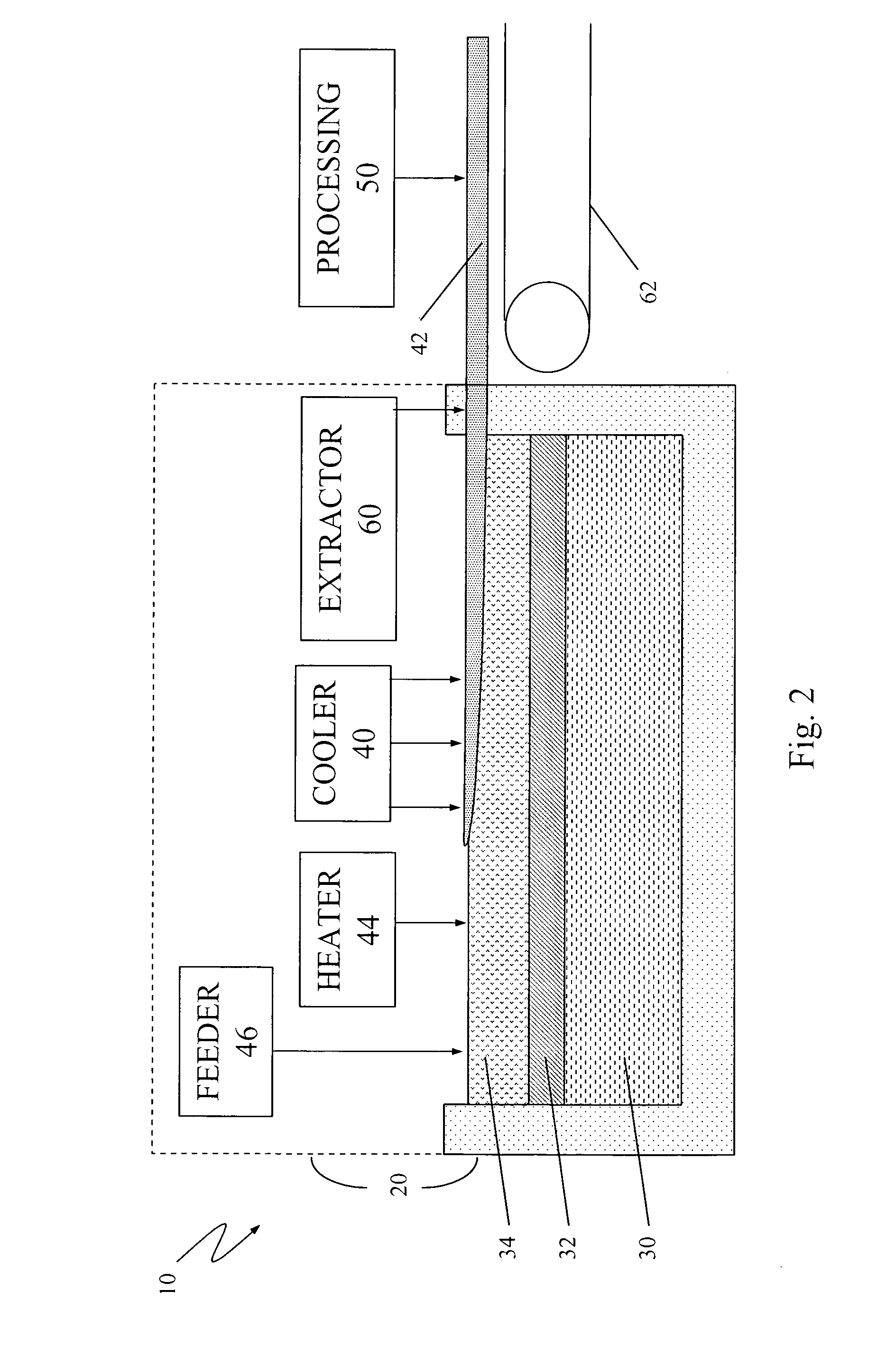
[0044]The present invention will generally be described in terms of manufacturing Silicon sheets suitable for solar cells by floating molten Silicon over “molten state substrate(s)” that comprises of high-density molten metals / alloys and silicate slags. However, the present invention has other applications and may be used, for example, with materials other than Silicon and the present invention may be used, for example, to make apparatuses other than solar cells. The present invention includes many modifications and variations, and the specific descriptions and embodiments provided herein are illustrative of the present invention and not limiting.

[0045]FIG. 1 illustrates one embodiment of an apparatus 10 according to the present invention. In that embodiment, the apparatus 10 includes a container 20 including first 30, second 32, and third 34 liquid layers. The present invention may also include a cooler 40, a heater 44, and a f...


PUM

PropertyMeasurementUnit
weight percentaaaaaaaaaa
thickaaaaaaaaaa
grain sizeaaaaaaaaaa

Abstract

A method for producing a solid layer material (42), comprising providing (70) a first layer (30); providing (72) a second liquid layer (32) on the first layer (30); providing (74) a third liquid layer (34) on the second liquid layer (32), wherein the third liquid layer has a melting point that is higher than a melting point of the second liquid layer, and wherein the second liquid layer is between the first and third layers; cooling (76) a surface of the third liquid layer to a temperature less than the melting point of the third liquid layer; forming (78) the solid layer from the third liquid layer while cooling the third layer liquid; and removing (80) the solid layer.

Description

CROSS-REFERENCE TO RELATED APPLICATIONS[0001]This application claims priority from U.S. Provisional Patent Application No. 61 / 199,238, filed Nov. 14, 2008, which is incorporated herein by reference.FIELD OF THE INVENTION[0002]The present invention is directed generally to methods for casting by a float process and for associated apparatuses and, for example, to such methods and apparatuses related to the production of silicon and solar cells.BACKGROUND OF THE INVENTION[0003]Many industries and products process semiconductors and semiconductor wafers into other products, such as microprocessors, computer memory, solar cells, and other devices. Semiconductor wafer have become a commodity in many cases, but the process of making wafers is still largely inefficient.[0004]In the conventional wafering process, multi-crystalline (mc) and single-crystalline (sc) Silicon (Si) wafers are obtained by unidirectional slicing of Silicon ingots. Such processes currently account for more than 90% o...

Claims


Application Information

Patent Timeline
Patent Type & Authority Applications(United States)
IPC IPC(8): C01B33/02C30B35/00C30B11/02
CPCB22D11/01C01B33/037C30B15/007C30B15/22C30B29/06C30B29/60C30B15/30Y02E10/546C30B15/14C30B15/002C30B15/28C30B15/06H01L31/182C30B29/64Y02P70/50
Inventor YDSTIE, BIRGER ERIKRANJAN, SUDHIRSUKUMAR, BALAJISEETHARAMAN, SRIDHAR
Owner CARNEGIE MELLON UNIV
Why Eureka
Try Eureka