Method to fabricate thin insulating film

a thin film, insulating technology, applied in the direction of vacuum evaporation coating, transistor, coating, etc., can solve the problems of affecting the performance of tft, affecting the performance of plasma processes, and expensive vacuum tools, etc., to achieve high quality

Inactive Publication Date: 2002-10-31
SEIKO EPSON CORP
View PDF0 Cites 13 Cited by
  • Summary
  • Abstract
  • Description
  • Claims
  • Application Information

AI Technical Summary

Benefits of technology

0006] The object of the present invention is to provide an inexpensive method for fabricating insulating films of high quality at low temperatures....

Problems solved by technology

The thermal oxidation process has undesirable side-effects such as redistribution of the dopant profiles in the semiconductors since significant diffusion of dopants occurs at high temperatures used in the this process.
Such devices require a SiO.sub.2 layer to be formed at a temperature below 430 degree C., as these displays use optically transparent substrate such as glass which can not withstand higher temperatures.
For such TFT applications, currently deposited SiO.sub.2 films are used which are of inf...

Method used


Image

  • Method to fabricate thin insulating film
  • Method to fabricate thin insulating film
  • Method to fabricate thin insulating film

Examples


example 2

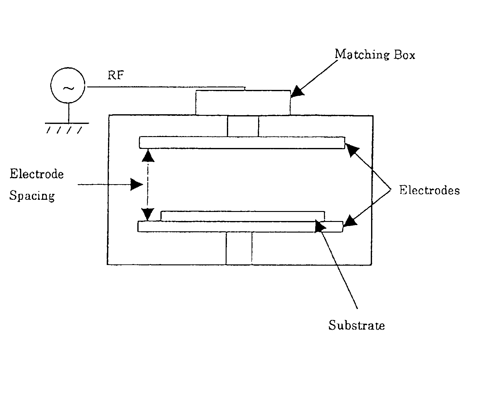
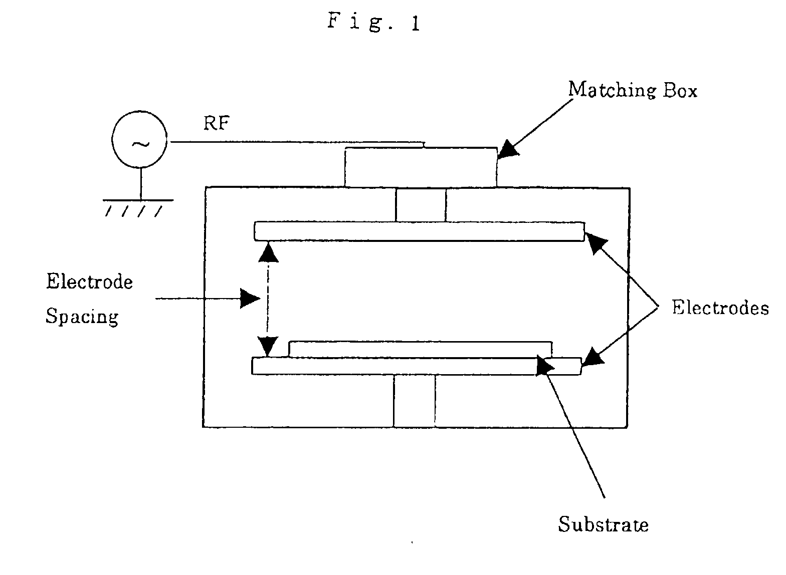
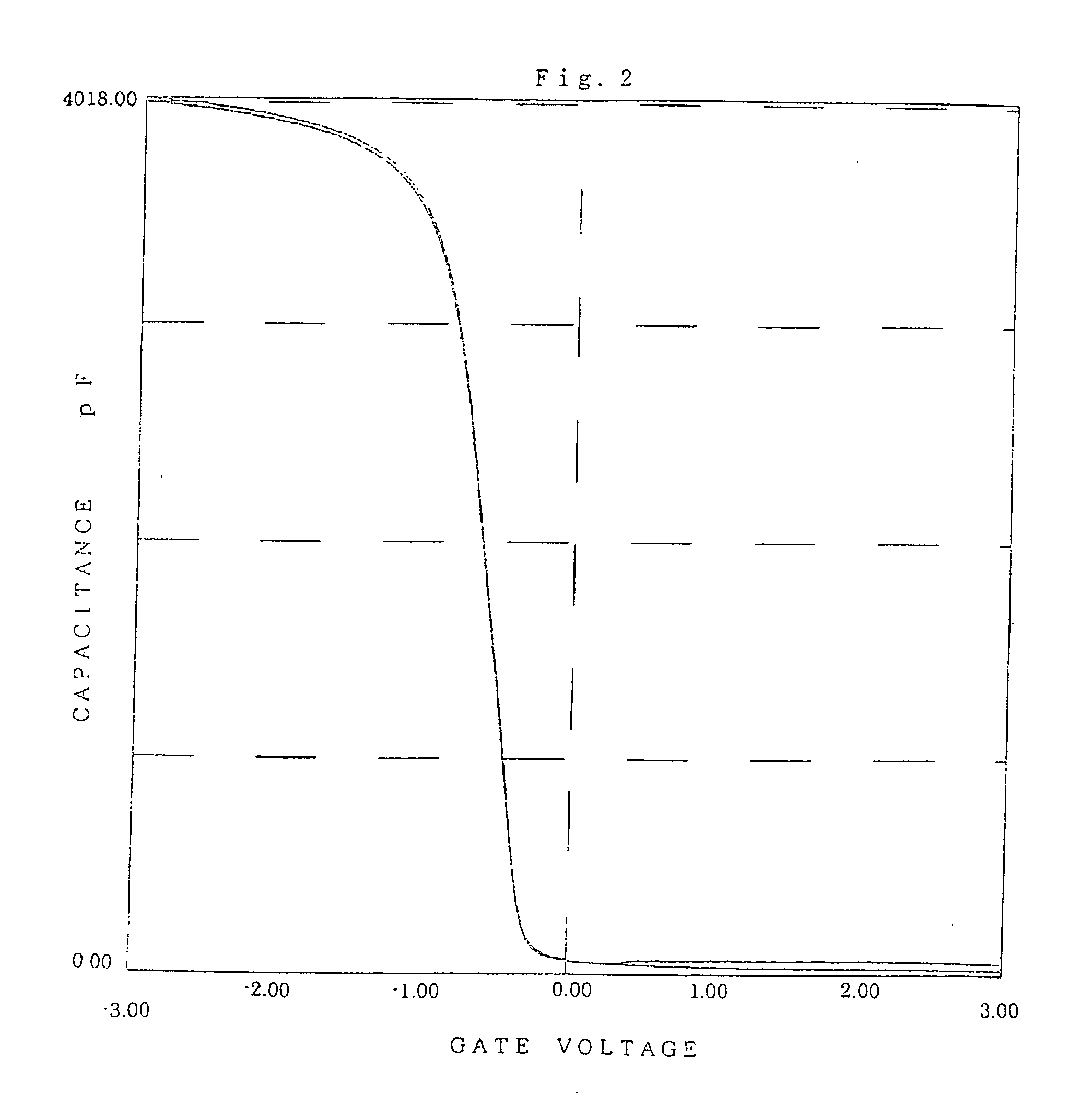
[0020] In the disclosed process of example 1, the silicon substrate to react with plasma was placed between the electrodes between which the plasma was created. It is possible to create plasma by applying RF power in a separate chamber and then transfer the plasma to another chamber in which a silicon substrate to react with the plasma is placed. Such process is called remote plasma process and is expected to reduce plasma damage to the substrate and further improve the quality of the SiO.sub.2 films. MOS capacitor were fabricated using the SiO.sub.2 films produced by remote plasma oxidation. For the SiO.sub.2 formation, the pressure was 1 atmosphere (about 100 kPa), the temperature was 200 .quadrature.{haeck over (Z)}, the O.sub.2 / He gas flow ratio was 1.5%, and the power density was 70 W / cm.sup.2. FIG. 3 shows the C-V characteristics of the MOS capacitor. In spite of using very high power density, no hysterysis is seen in FIG. 3, showing low damage to SiO.sub.2 films by remote pla...

example 3

[0025] The SiO.sub.2 film produced by the disclosed process was incorporated in the fabrication process of TFTs. Two kinds of TFTs were fabricated. 1. Reference TFTs, which were fabricated by a routine TFT process and 2. Plasma oxidation TFTs, which were fabricated by the following steps, of which step 3 includes one of the methods related to the present invention.

[0026] 1. On a glass substrate, amorphous silicon layer with a thickness of 50 nm was deposited by LPCVD method.

[0027] 2. The amorphous silicon films was laser annealed by a XeCl pulsed laser to change it in to polycrystalline silicon with an approximate grain size of 0.3 micrometers, and the polycrystalline silicon layer was subsequently patterned by photolithography to make islands.

[0028] 3. An SiO.sub.2 layer (SiO.sub.2 layer 1) with a thickness of 4 nm was fabricated over the polycrystalline silicon applying RF power to oxygen-helium gas mixture at pressure substantially close to 1 atmosphere (about 100 kPa). An SiO.su...


PUM

PropertyMeasurementUnit
Lengthaaaaaaaaaa
Fractionaaaaaaaaaa
Fractionaaaaaaaaaa

Abstract

In this disclosure, we present processes of growing SiO2 films over silicon at temperatures as low as room temperature and at pressures as high as 1 atmosphere. The lower temperature oxidation was made possible by creation of oxygen atoms and radicals by adding noble gas(es) along with oxidizing gas(es) and applying RF power to create plasma. It was also possible to fabricate silicon nitride films by flowing nitrogen containing gas(es) with noble gas(es) and applying RF power to create plasma at pressures as high as one atmosphere. In addition, the above processes could also be carried out using microwave power instead of RF power to create plasma.

Description

[0001] The present invention relates to a method of fabricating insulating films for application in to thin film transistors (TFTs) and metal insulator oxide (MOS) transistors.[0002] A process for forming an insulating film such as SiO.sub.2 is one of key processes for manufacturing transistors such as silicon MOSFET (Metal Oxide Semiconductor Field Effect Transistor). Formation of SiO.sub.2 film on silicon is carried out at temperatures usually higher than 1000 degree C. in the presence of chemical species that oxidize the silicon. This process is known as thermal oxidation. The thermal oxidation process has undesirable side-effects such as redistribution of the dopant profiles in the semiconductors since significant diffusion of dopants occurs at high temperatures used in the this process.[0003] Thin film transistor (TFT) devices, which have a basic structure similar to that of a usual MOSFET, have been used for display applications such as liquid crystal display (LCD) and organic...

Claims


Application Information

Patent Timeline
IPC IPC(8): H01L21/28H01L21/316H01L29/78H01L21/318H01L21/321H01L21/336H01L29/51H01L29/786
CPCH01L21/02238H01L21/02252H01L21/28158H01L21/28185H01L21/28202H01L29/66757H01L21/31662H01L21/3185H01L21/32105H01L29/518H01L21/28211C23C14/10
Inventor KAKKAD, RAMESH H.
Owner SEIKO EPSON CORP
Why Eureka
Try Eureka