Semiconductor device
a technology of semiconductor devices and semiconductors, applied in the direction of semiconductor devices, electrical equipment, transistors, etc., can solve the problems of delayed commercialization of semiconductor devices using silicon carbide, difficult melting of silicon carbide, etc., and achieve the effects of reducing the cost of silicon carbid
- Summary
- Abstract
- Description
- Claims
- Application Information
AI Technical Summary
Benefits of technology
Problems solved by technology
Method used
Image

Examples
embodiment 1
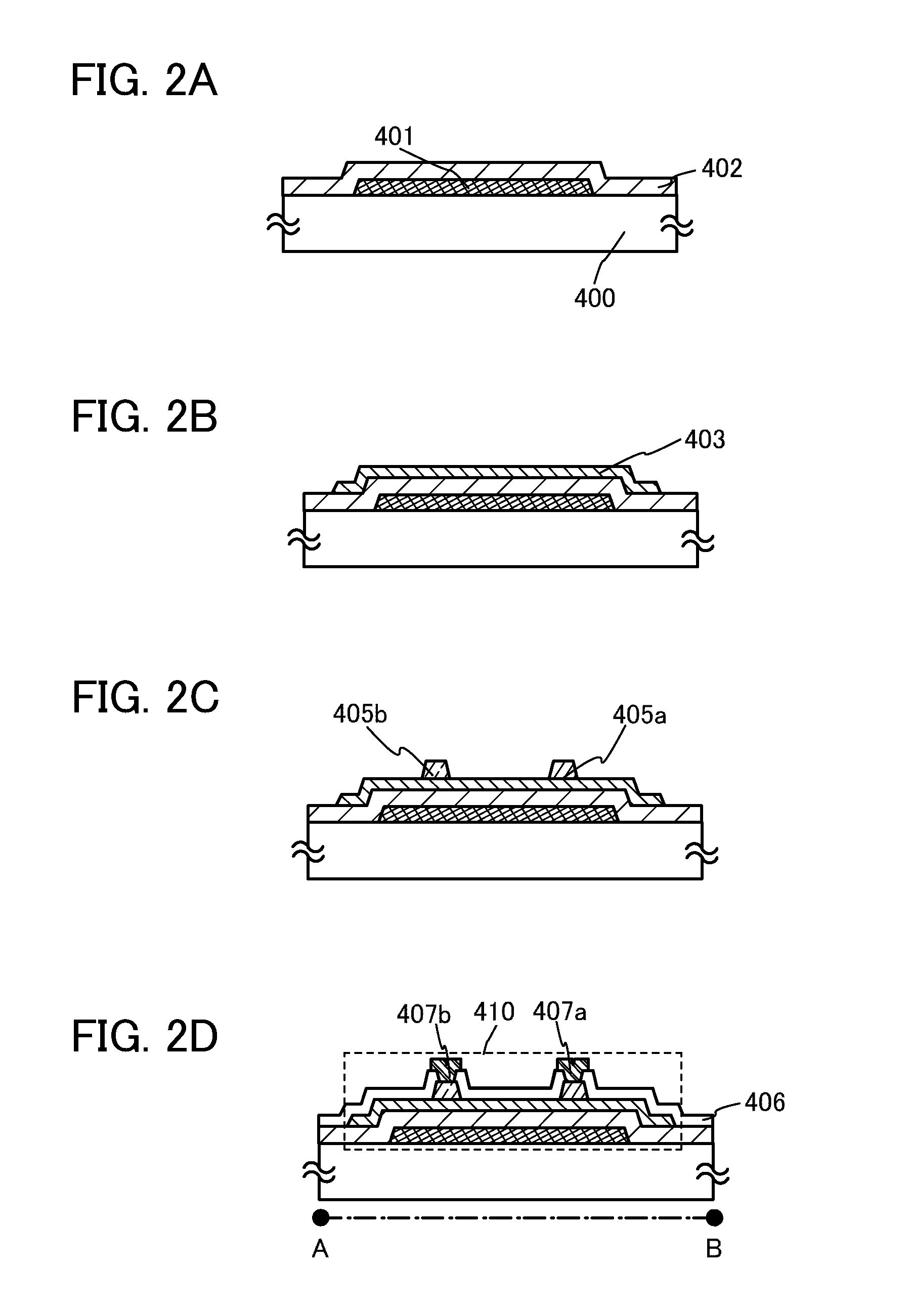
[0035]In this embodiment, one embodiment of a semiconductor device and a method for manufacturing the semiconductor device will be described with reference to FIGS. 1A to 1C, FIGS. 2A to 2D, FIGS. 3A to 3C, and FIGS. 4A and 4B.
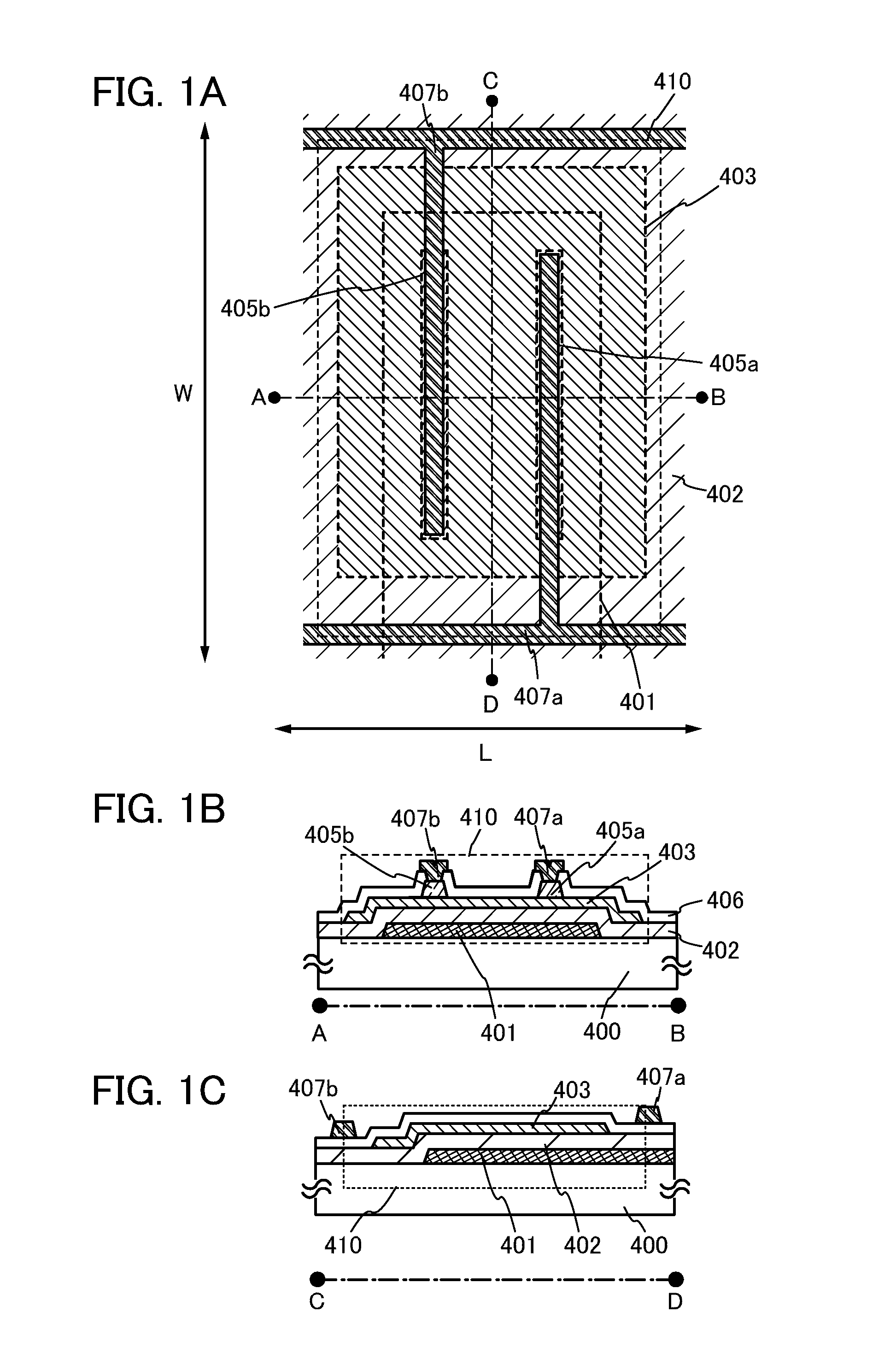
[0036]FIG. 1A is a plan view of a transistor 410. FIG. 1B is a cross-sectional view taken along line A-B in FIG. 1A. FIG. 1C is a cross-sectional view taken along line C-D in FIG. 1A.
[0037]The transistor 410 illustrated in FIGS. 1A to 1C includes, over a substrate 400, a gate electrode 401, a gate insulating layer 402 covering the gate electrode 401, an oxide semiconductor layer 403 provided over the gate insulating layer 402, a first source electrode 405a and a first drain electrode 405b provided in contact with the oxide semiconductor layer 403, an insulating layer 406 covering the oxide semiconductor layer 403, the first source electrode 405a, and the first drain electrode 405b, and a second source electrode 407a and a second drain electrode 407b provided o...
modification example
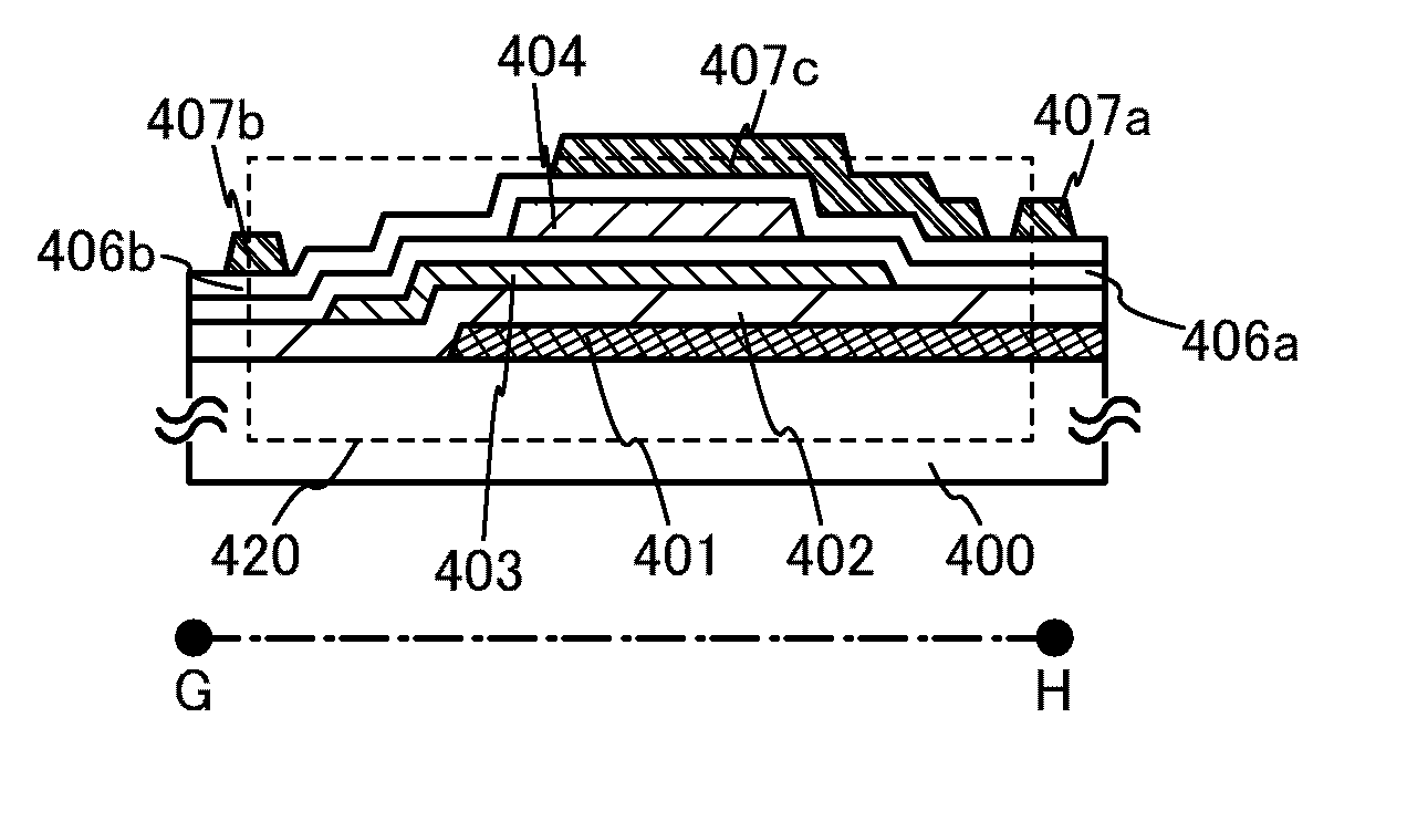
[0083]Next, another structure of the semiconductor device illustrated in FIGS. 1A to 1C will be described with reference to FIGS. 3A to 3C.
[0084]FIG. 3A is a plan view of a transistor 420. FIG. 3B is a cross-sectional view taken along line E-F in FIG. 3A. FIG. 3C is a cross-sectional view taken along line G-H in FIG. 3A.
[0085]The transistor 420 illustrated in FIGS. 3A to 3C includes, over the substrate 400, the gate electrode 401, the gate insulating layer 402 covering the gate electrode 401, the oxide semiconductor layer 403 provided over the gate insulating layer 402, the first source electrode 405a and the first drain electrode 405b provided in contact with the oxide semiconductor layer 403, a first insulating layer 406a covering the oxide semiconductor layer 403, the first source electrode 405a, and the first drain electrode 405b, a first conductive layer 404 provided over the first insulating layer 406a, a second insulating layer 406b covering the first conductive layer 404, an...
embodiment 2
[0107]In this embodiment, a structure of a semiconductor device different from that described in Embodiment 1 will be described with reference to FIGS. 5A and 5B, FIGS. 6A and 6B, and FIGS. 7A and 7B. Note that detailed description of the portion same as or a portion having a function similar to that in Embodiment 1 is omitted.
[0108]FIG. 5A is a plan view of a transistor 450 and FIG. 5B is a cross-sectional view taken along line I-J in FIG. 5A.
[0109]The transistor 450 illustrated in FIGS. 5A and 5B includes, over the substrate 400, the gate electrode 401, the gate insulating layer 402 covering the gate electrode 401, the oxide semiconductor layer 403 provided over the gate insulating layer 402, a plurality of first source electrodes 405a (three first source electrodes 405a in FIGS. 5A and 5B) and a plurality of first drain electrodes 405b (four first drain electrodes 405b in FIGS. 5A and 5B) provided in contact with the oxide semiconductor layer 403, the insulating layer 406 coverin...
PUM
 Abstract
Description
Claims
Application Information