Method for manufacturing metal laminated substrate for semiconductor element formation and metal laminated substrate for semiconductor element formation

a technology of metal laminated substrates and semiconductor elements, which is applied in the direction of metallic pattern materials, chemically reactive gases, crystal growth processes, etc., can solve the problems of high cost of ni—w alloys, difficult handling of monocrystalline wafers made of si or the like during the conveyance of wafers, and inability to form monocrystalline wafers by continuous manufacturing methods such as reel-to-reel methods, etc., to achieve low cost, high thickness accuracy, and high reduction

Inactive Publication Date: 2011-12-01
TOYO KOHAN CO LTD
View PDF5 Cites 8 Cited by
  • Summary
  • Abstract
  • Description
  • Claims
  • Application Information

AI Technical Summary

Benefits of technology

[0026]According to the method of manufacturing a metal laminated substrate for forming a semiconductor element of the present invention, a metal plate and a Cu alloy foil rolled at a high rolling reduction for obtaining a metal crystal orientation surface which are manufactured with high thickness accuracy respectively in advance can be laminated to each other at a low rolli

Problems solved by technology

However, the monocrystalline wafer made of these materials is a cut plate having a size of approximately 300 mmφ at most, and such a monocrystalline wafer cannot be formed by a continuous manufacturing method such as a reel-to-reel method.
Further, also the strength of Si or the like is small and hence, the handling of the monocrystalline wafer made of Si or the like during the conveyance of the wafer is not easy whereby the careful handling of the wafer is necessary.
Further, the above-mentioned Ni—W alloy has drawbacks that the Ni—W alloy is not a material which is used popularly in general so that a cost of the Ni—W alloy is high, the Ni—W alloy exhibits poor workability so that the manufacture of the substrate having a large width becomes difficult.
Although it has been known that working efficiency of 90% or more is necessary to impart the high crystal orientation to an Ni layer after diffusion heat treatment, when stron

Method used


Image

  • Method for manufacturing metal laminated substrate for semiconductor element formation and metal laminated substrate for semiconductor element formation
  • Method for manufacturing metal laminated substrate for semiconductor element formation and metal laminated substrate for semiconductor element formation
  • Method for manufacturing metal laminated substrate for semiconductor element formation and metal laminated substrate for semiconductor element formation

Examples


example 1

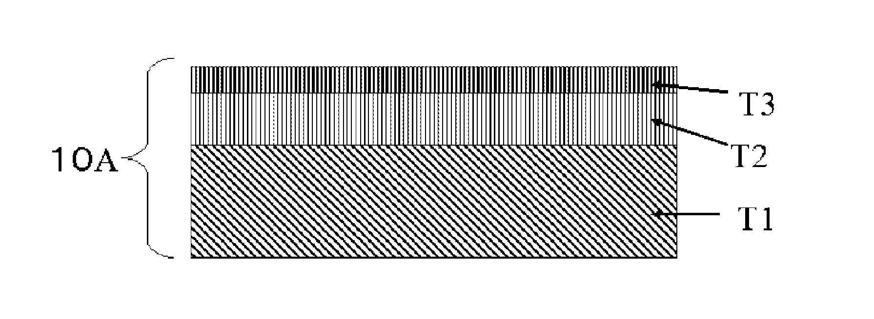
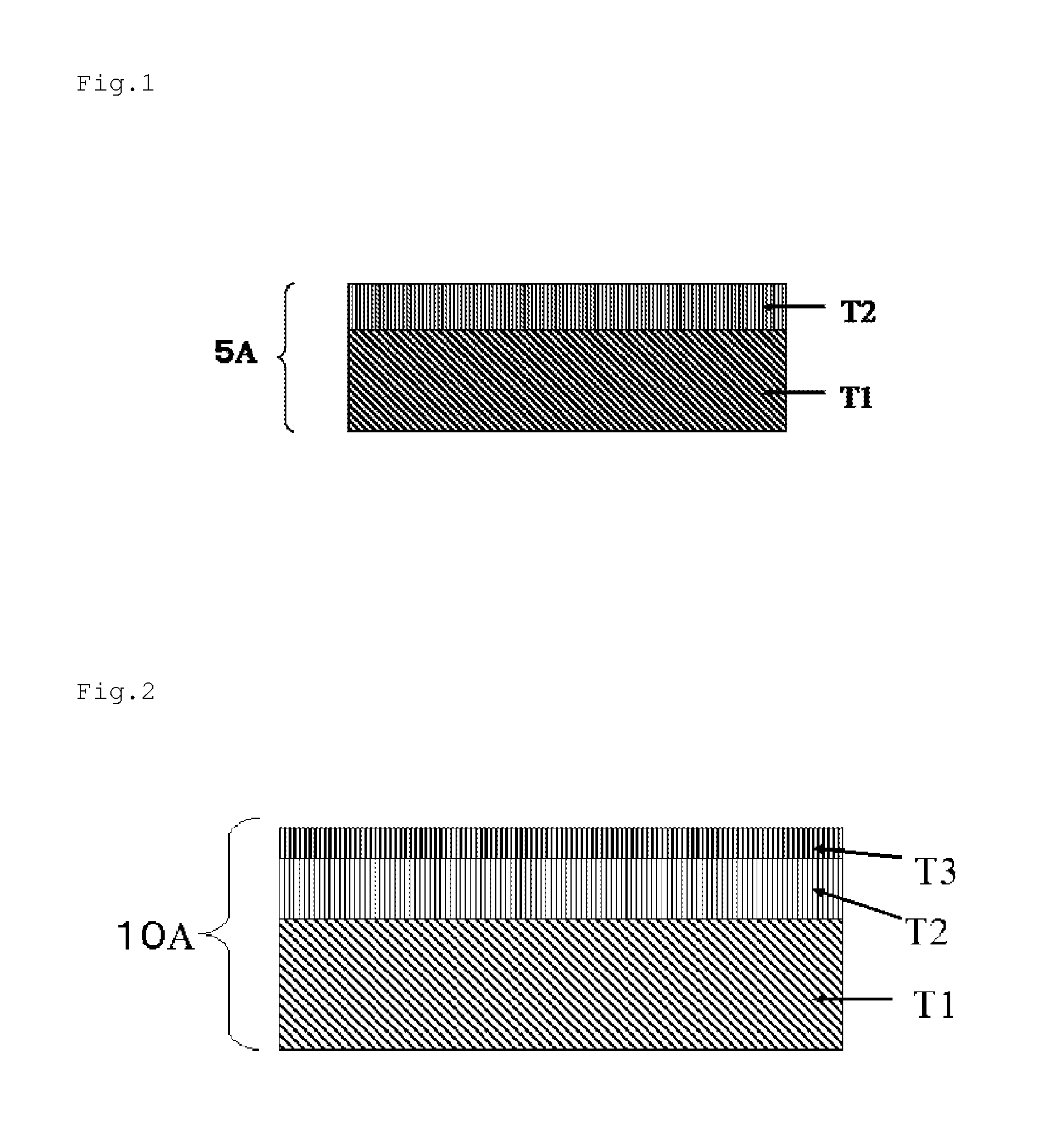
[0071]Hereinafter, an embodiment of the present invention is exemplified, wherein properties of the manufactured metal laminated substrate are explained. A high-reduction rolled Cu foil (metal foil) having a width of 200 mm and a thickness of 18 μm and an SUS316L plate (metal plate) having a thickness of 100 μm are bonded to each other by a room-temperature surface activation bonding method and, thereafter, the high-reduction rolled Cu foil and the SUS316L plate are subjected to heat treatment at a temperature of 200° C. to 1000° C. for five minutes thus acquiring the metal laminated substrate.

[0072]Table 1 shows a rate at which a Cu (200) surface is made parallel to a Cu foil surface, that is, a crystal orientation rate (a diffraction peak strength rate of a (200) surface at a θ / 2θ diffraction peak measured by X-ray diffraction: I(200) / ΣI(hkl)×100(%)), and a Δφ° (φ scan peak (an average value of half value widths of 4 peaks at α=35°) obtained by an Ni (111) pole figure in accordanc...


PUM

PropertyMeasurementUnit
Temperatureaaaaaaaaaa
Fractionaaaaaaaaaa

Abstract

Disclosed is a metal laminated substrate for forming an epitaxial growth film for forming a semiconductor element having high biaxial crystal orientation on a surface of a metal substrate and a method of manufacturing the metal laminated substrate. The manufacturing method includes the steps of activating at least one surface of a metal plate T1 by sputter etching or the like; activating at least one surface of a metal foil T2 made of Cu or a Cu alloy which is cold-rolled at a rolling reduction of 90% or more; laminating the metal plate and the metal foil such that an activated surface of the metal plate and an activated surface of the metal foil face each other in an opposed manner and applying cold rolling to the metal plate and the metal foil which are laminated to each other at a rolling reduction of 10% or less, for example; and biaxially orienting crystals of the metal foil by heat treatment at a temperature of not lower than 150° C. and not higher than 1000° C.

Description

TECHNICAL FIELD[0001]The present invention relates to a method of manufacturing a metal laminated substrate for forming an epitaxial growth film for forming a semiconductor element, and a metal laminated substrate for forming an epitaxial growth film for forming a semiconductor element.BACKGROUND ART[0002]To obtain an excellent semiconductor element, it is necessary to form an epitaxial growth film having high orientation on a substrate.[0003]For this end, conventionally, as a substrate for an epitaxial growth film, a monocrystalline wafer made of monocrystalline silicon (Si), monocrystalline GaAs, monocrystalline sapphire (Al2O3) or the like having an excellent crystal orientation has been used.[0004]However, the monocrystalline wafer made of these materials is a cut plate having a size of approximately 300 mmφ at most, and such a monocrystalline wafer cannot be formed by a continuous manufacturing method such as a reel-to-reel method. Further, also the strength of Si or the like i...

Claims


Application Information

Patent Timeline
IPC IPC(8): C22F1/08C23F1/00C22C9/00
CPCB32B15/01B32B15/015H01L2924/0002C22C9/00C22C38/02C22C38/44C22C38/58C22F1/08C30B25/18C30B29/06C30B29/16C30B29/40C30B29/52C30B33/00H01L23/142H01L31/03921H01L33/007H05K1/0393H05K1/09H05K3/022H05K2201/0355H05K2203/1105Y02E10/50H01L2924/00B21B47/00H01L21/20
Inventor OKAYAMA, HIRONAOKANEKO, AKIRANANBU, KOUJI
Owner TOYO KOHAN CO LTD
Why Eureka
Try Eureka