Method for manufacturing insulated conductive pattern and laminate

Active Publication Date: 2011-12-01
LG CHEM LTD
View PDF2 Cites 6 Cited by
  • Summary
  • Abstract
  • Description
  • Claims
  • Application Information

AI Technical Summary

Benefits of technology

[0015]According to the exemplary embodiments of the present invention, since a separate photoresist material and a stripping solution for forming a conductive pattern are not used, there are no problems of an increase in cost and an environmental pollution, and since a process is simple as compared to a known photolithography process, there is an economic efficiency. In addition, since

Problems solved by technology

The known process does not use a constitutional element of the conductive pattern but uses a photoresist material and a stripping solution, thereby increasing a process cost due to a cost of the photoresist material and the stripping solution and a cost of removal the photoresist material and the stripping solution.
In addition, there is a pro

Method used


Image

  • Method for manufacturing insulated conductive pattern and laminate
  • Method for manufacturing insulated conductive pattern and laminate
  • Method for manufacturing insulated conductive pattern and laminate

Examples


example 1

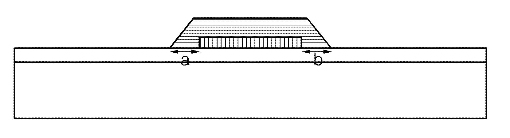
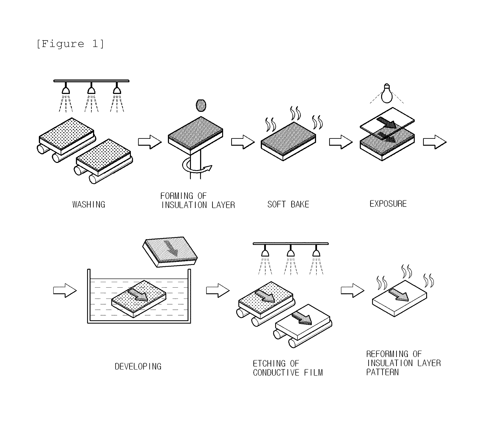
[0092]The chrome layer having the thickness of 300 nm was formed as the conductive film on the glass substrate by the deposition method. Subsequently, the insulation layer pattern having the width of 60 micrometers and the pitch of 5 mm was formed by adding the novolac resin composition (trade mark: LG412DF, manufactured by LG Chem, Ltd., in Korea) on the chrome layer by using the photolithography method. The soft bake was performed in respects to the insulation layer by maintaining the temperature at 107° C. during the process for forming the insulation layer pattern by using the photolithography method.

[0093]The chrome layer was patterned by using the insulation layer pattern as the mask. In this case, trade mark CE-05E manufactured by EXAX, Co., Ltd., in Korea was used as the etching solution. The width of the upper part of the chrome layer pattern manufactured by the method was 57 micrometers and the taper angle was 18°.

[0094]The substrate including the insulation layer pattern ...

example 2

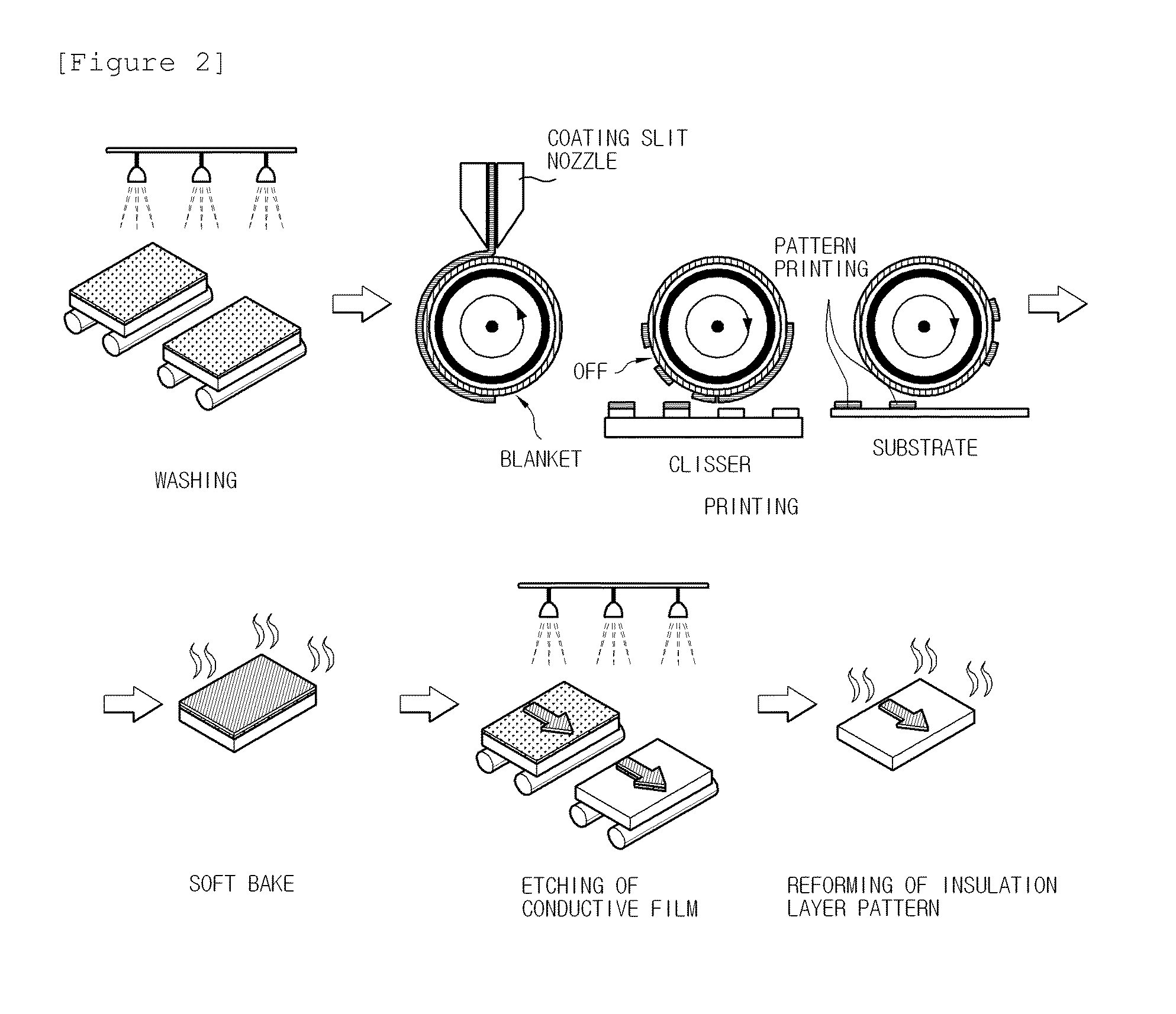
[0095]The same method as Example 1 was performed, except that LG412DF to which the surfactant was added and the PGMEA / EtOH mixed solvent (mixing weight ratio 7:3) were mixed in the solid content of 13 wt % and used as the material of the insulation layer pattern, and the reverse offset printing method was used instead of the photolithography method as the method for forming the insulation layer pattern. The electronic microscopic pictures of the upper surface and the lateral surface of the resultant material formed by this are shown in FIG. 5.

example 3

[0096]The same method as Example 1 was performed, except that silver was used instead of chrome as the material of the conductive film. The reflow shape as shown in FIG. 4 and measured in Example 1 could be obtained.


PUM

PropertyMeasurementUnit
Fractionaaaaaaaaaa
Angleaaaaaaaaaa
Angleaaaaaaaaaa

Abstract

The present invention provides: a method for manufacturing an insulated conductive pattern, wherein a conductive film and an insulation layer pattern are formed on a substrate, and the insulation layer pattern is reformed to cover a conductive pattern after formation of the conductive pattern by etching the conductive film using the insulation layer pattern as a mask; and a laminate manufactured thereby. According to the present invention, the number of processes is sharply reduced in comparison with the existing processes, and economic efficiency can be greatly improved.

Description

DISCLOSURE[0001]1. Technical Field[0002]The present invention relates to a method for manufacturing an insulated conductive pattern and laminate. This application claims priority from Korean Patent Application Nos. 10-2009-0009750, 10-2009-0127756, 10-2009-0127757 and 10-2009-0127759 filed on Feb. 6, 2009 and Dec. 21, 2009 in the KIPO, the disclosure of which is incorporated herein by reference in their entirety.[0003]2. Background Art[0004]A process for manufacturing a known general conductive pattern is as follows. First, a photoresist pattern is formed by uniformly coating photoresist on a conductive film formed on a substrate and selectively exposing and developing the photoresist. Subsequently, the conductive pattern is transferred on a lower layer of the photoresist by etching the conductive film by using the patterned photoresist pattern as a mask. Thereafter, the unnecessary photoresist layer is removed by a stripping solution. Subsequently, an insulation layer is uniformly ...

Claims


Application Information

Patent Timeline
IPC IPC(8): H05K1/11H05K3/22H05K3/06
CPCH05K3/061H05K3/064H05K2203/1184H05K2201/09827H05K2203/0571H05K3/28C23F1/02H05K1/0296
Inventor HWANG, JI-YOUNGMIN, SUNG-JOONHWANG, IN-SEOKLEE, DONG-WOOKCHUN, SANG-KI
Owner LG CHEM LTD
Why Eureka
Try Eureka