Integrated circuit with timing adjustment mechanism

a timing adjustment mechanism and integrated circuit technology, applied in the direction of specific program execution arrangements, multi-port active networks, program control, etc., can solve the problems of inability to operate correctly, critical paths operating either too quickly or too slowly, and the integrated circuit concerned cannot function correctly, so as to reduce the overhead associated with the present technique and improve the robustness of the control of the variable delay circuitry

Active Publication Date: 2011-12-01
ARM LTD
View PDF15 Cites 2 Cited by
  • Summary
  • Abstract
  • Description
  • Claims
  • Application Information

AI Technical Summary

Benefits of technology

[0016]While one possibility is to provide a separate regulated current line for each individual variable delay circuitry, the amount of overhead associated with the present technique may be reduced when a regulated current line is shared using time division multiplexing between a plurality of variable delay circuitry with each of these being coupled to the regulated current line via a respective transmission gate. Thus, within respective time slots of the time division multiplexing, each variable delay circuitry can have its additional delay amount adjusted using the regulated current line and when other variable delay circuitry is being adjusted may be isolated from the regulated current line using a transmission gate.
[0017]The robustness of the control of the variable delay circuitry may be improved by the provision of analog buffer circuitry configured to receive the control voltage as an input signal and to output a buffered signal which is then used to control the additional delay amount.
[0018]As the control voltage used to control operation of the variable delay circuitry will typically be less than a full rail voltage, this may not be well suited to controlling propagation of both rising and falling edges of the processing signal. Accordingly, in some embodiments the variable delay circuitry is configured to use the control voltage to control switching of a first transistor within an inverter to drive an output of the inverter corresponding to the processing signal when the processing signal has a first value and to use a power supply voltage to control switching of a second transistor within the inverter to drive the output of the inverter corresponding to the processing signal when the processing signal has a second value. Thus, the use of less than fall rail control voltages to control the switching of inventor may be avoided in circumstances where it is not desired.

Problems solved by technology

Such critical paths may, for example, represent processing bottlenecks which restrict the maximum processing speed which can be achieved if they operate too slowly, or may be paths, such as timing paths used within self-timed circuits, which will cause incorrect operation if they operate too quickly.
Thus, while an integrated circuit may be designed such that the critical paths have a typical path delay which will produce correct operation, the variations produced in manufacturing may mean that some of these critical paths operate either too quickly or too slowly and the integrated circuit concerned will not function correctly.
This reduces the yield of correctly operating integrated circuits produced by the manufacturing process.
These problems are becoming greater as process geometry sizes are reducing since the degree of variation due to manufacturing increases at smaller process geometry sizes.
There is a further problem that the ageing of integrated circuits can change path delays and take these outside an acceptable range causing the integrated to fail when in use.

Method used


Image

  • Integrated circuit with timing adjustment mechanism
  • Integrated circuit with timing adjustment mechanism
  • Integrated circuit with timing adjustment mechanism

Examples


Embodiment Construction

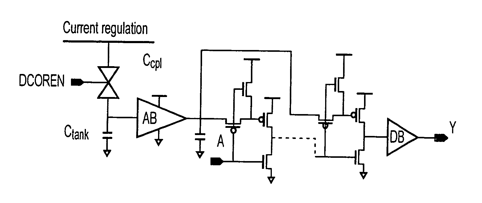
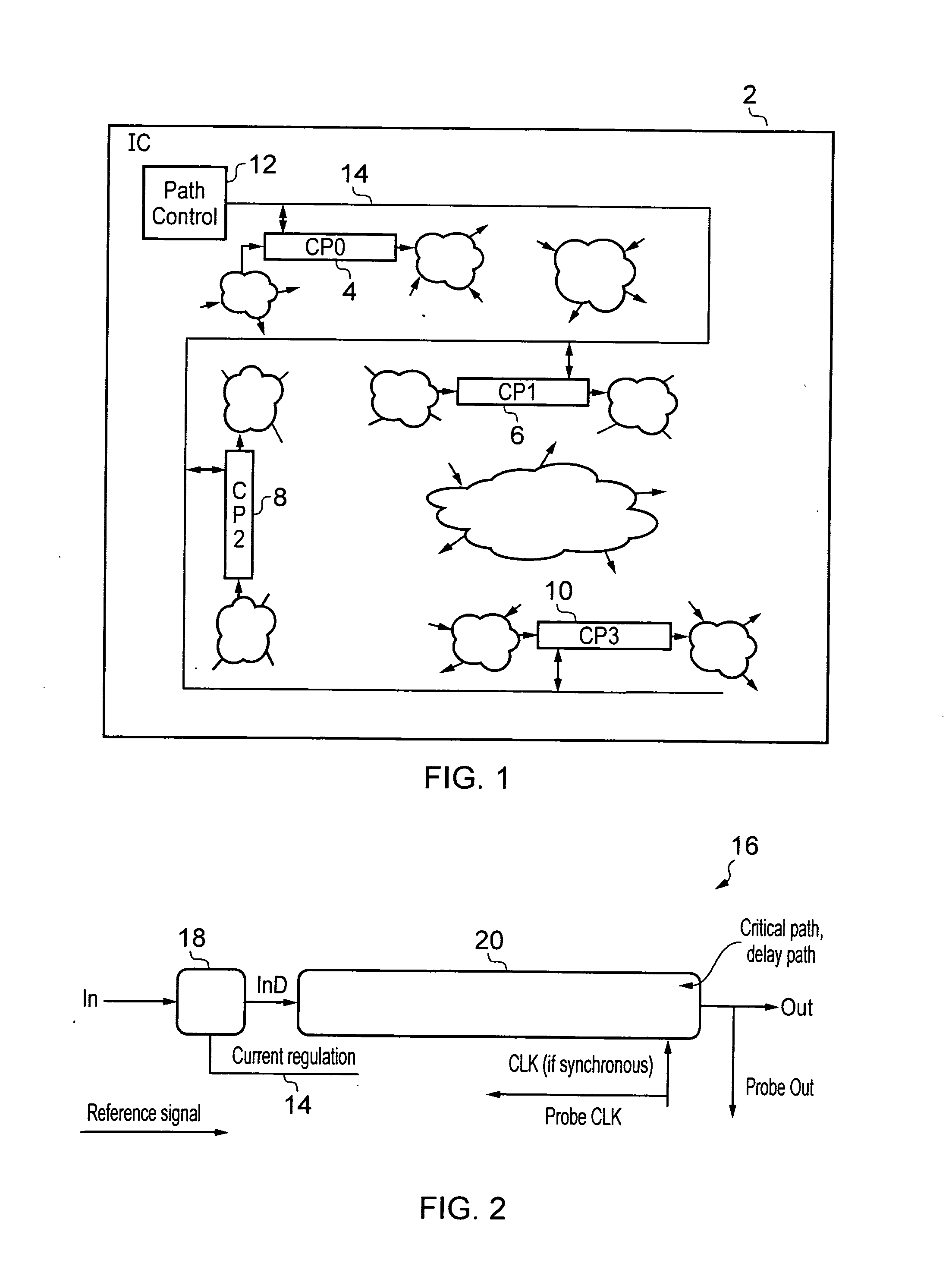
[0049]FIG. 1 schematically illustrates an integrated circuit 2 including processing circuitry for performing processing operations. This processing circuitry includes critical path circuits 4, 6, 8, 10 which each perform part of functional data processing operations of the integrated circuit. The critical path circuits 4, 6, 8, 10 may, for example, be timing paths used to generate self-timing signals within a memory circuit. Many other different forms of critical path circuit are also possible and the present techniques may be used with these different forms of critical path circuit.

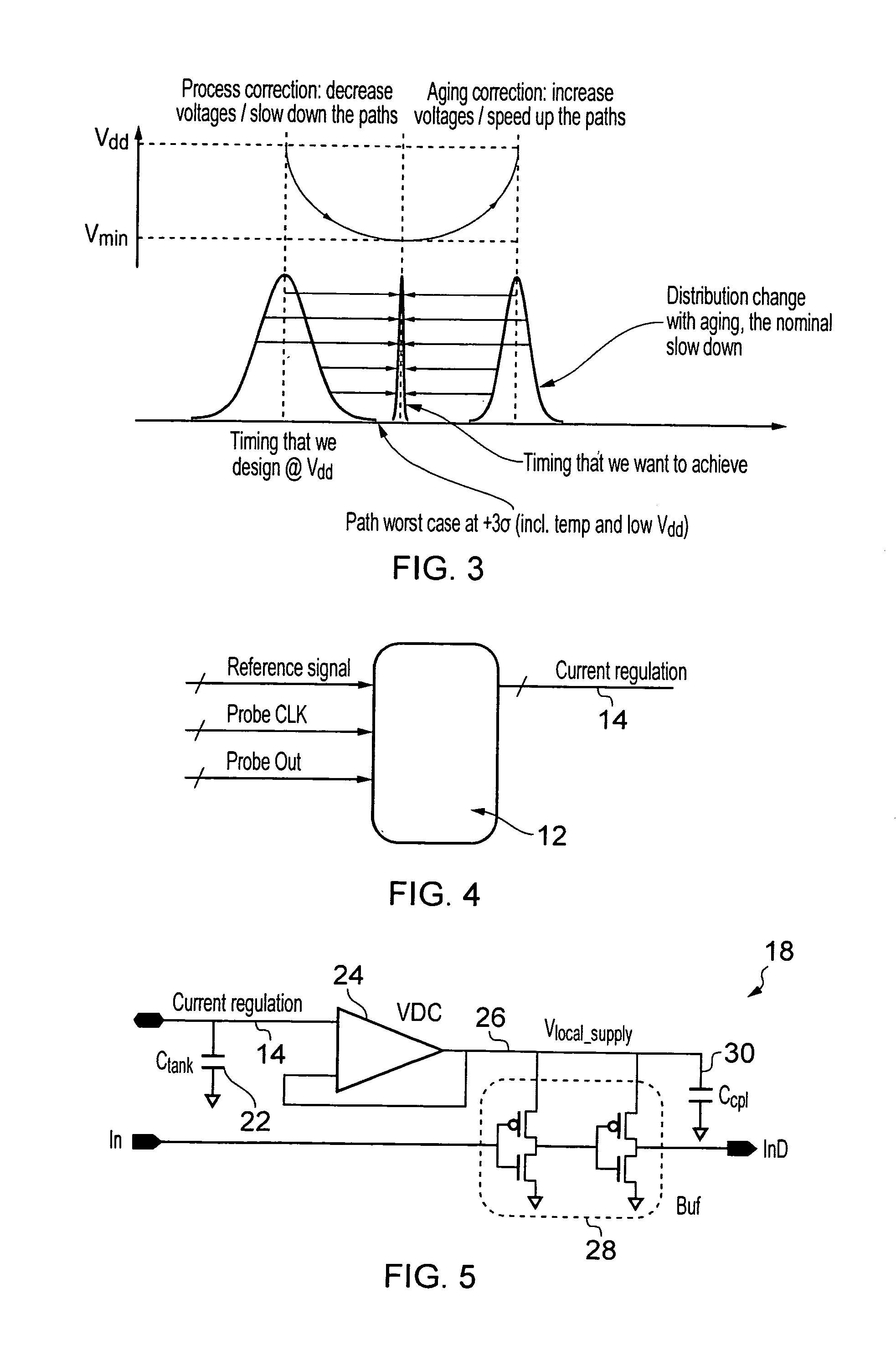
[0050]Path control circuitry 12 is coupled via a regulated current line 14 to each of the critical path circuits 4, 6, 8, 10. This regulated current line 14 is used to adjust an additional time delay that is part of the path delay of each of the critical path circuits 4, 6, 8, 10 and is provided by variable delay circuitry disposed within those critical path circuits 4, 6, 8, 10. Individual regulated cur...


PUM


Abstract

An integrated circuit 2 includes processing circuitry that includes a plurality of critical path circuits 4, 6, 8, 10. These critical path circuits include variable delay circuits 16 which add an additional delay in to the path delay through the critical paths so as to adjust the path delay to match a target path delay. Variable delay circuit 18 includes a tank capacitor 22 which is charged or discharged to generate a control voltage. This control voltage serves to control a power supply voltage fed to an inverter chain 28. Variation in the power supply voltage of the inverter chain 28 adjust the propagation speed of a processing signal through the inverter chain 28 and accordingly adjusts the additional delay imposed by the variable delay circuit.

Description

BACKGROUND OF THE INVENTION[0001]1. Field of the Invention[0002]This invention relates to the field of integrated circuits. More particularly, this invention relates to the timing constraints associated with signals propagating through an integrated circuit.[0003]2. Description of the Prior Art[0004]It is known within integrated circuits that certain portions of the integrated circuit represent critical paths for processing signals. Such critical paths may, for example, represent processing bottlenecks which restrict the maximum processing speed which can be achieved if they operate too slowly, or may be paths, such as timing paths used within self-timed circuits, which will cause incorrect operation if they operate too quickly. Existing circuit design and synthesis tools are able to identify such critical paths and simulate their operation to determine their typical, lowest and highest path delay when the integrated circuit is manufactured.[0005]It will be appreciated that variatio...

Claims


Application Information

Patent Timeline
Patent Type & Authority Applications(United States)
IPC IPC(8): H03H11/26
CPCH03H11/265H03K2005/00032H03K5/133H03K5/06
Inventor JAVERLIAC, VIRGILE
Owner ARM LTD
Why Eureka
Try Eureka