Manufacturing method and apparatus for a copper indium gallium diselenide solar cell

a manufacturing method and technology of copper indium gallium diselenide, applied in the field of thin film solar cells, can solve the problems of residual contamination of films, unfavorable use of zinc (“zn”) or cadmium, unintentional n-type doping of entirs, etc., to improve voc and solar conversion efficiency, reduce cost and problems, and improve the effect of solar cell performan

Inactive Publication Date: 2011-12-08
RJM SEMICON
View PDF0 Cites 11 Cited by
  • Summary
  • Abstract
  • Description
  • Claims
  • Application Information

AI Technical Summary

Benefits of technology

[0025]Yet another object of the invention is to eliminate the cost and problems related to disposal of toxic Cd containing baths typically used to deposit CdS buffer layers in CIGS solar cells.
[0026]A further object of the invention is to provide a buried p-n homojunction in CIGS to avoid impurity contamination including O and C at the CIGS surface due to atmospheric exposure, which can degrade solar cell performance.
[0027]Yet another object of the invention is to improve Voc and solar conversion efficiency by eliminating p-n junction interface recombinat

Problems solved by technology

However, it is not deemed feasible to use Zinc (“Zn”) or Cadmium (“Cd”) atoms to produce CIGS p-n junctions in a vacuum system due to the exceedingly high vapor pressure of these elements.
It is well known that Zn or Cd atoms introduced in a vacuum system will lead to persistent background pressures of these elements leading to residual contamination in films, which are not intentionally doped with

Method used


Image

  • Manufacturing method and apparatus for a copper indium gallium diselenide solar cell
  • Manufacturing method and apparatus for a copper indium gallium diselenide solar cell
  • Manufacturing method and apparatus for a copper indium gallium diselenide solar cell

Examples


Embodiment Construction

[0038]The invention may be understood more readily by reference to the following detailed description of preferred embodiment of the invention. However, techniques, systems and operating structures in accordance with the invention may be embodied in a wide variety of forms and modes, some of which may be quite different from those in the disclosed embodiment. Consequently, the specific structural and functional details disclosed herein are merely representative, yet in that regard, they are deemed to afford the best embodiment for purposes of disclosure and to provide a basis for the claims herein, which define the scope of the invention. It must be noted that, as used in the specification and the appended claims, the singular forms “a”, “an”, and “the” include plural referents unless the context clearly indicates otherwise.

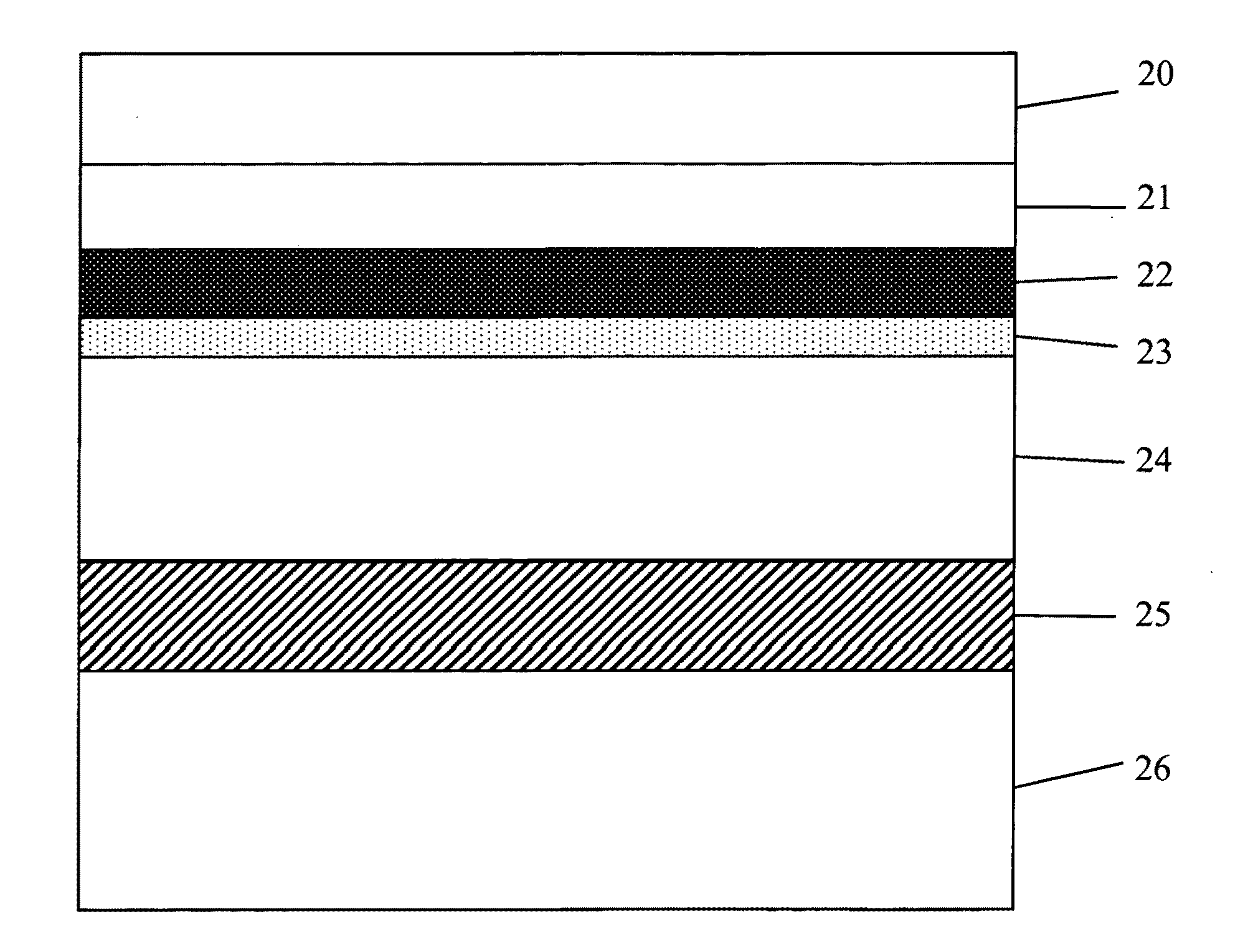
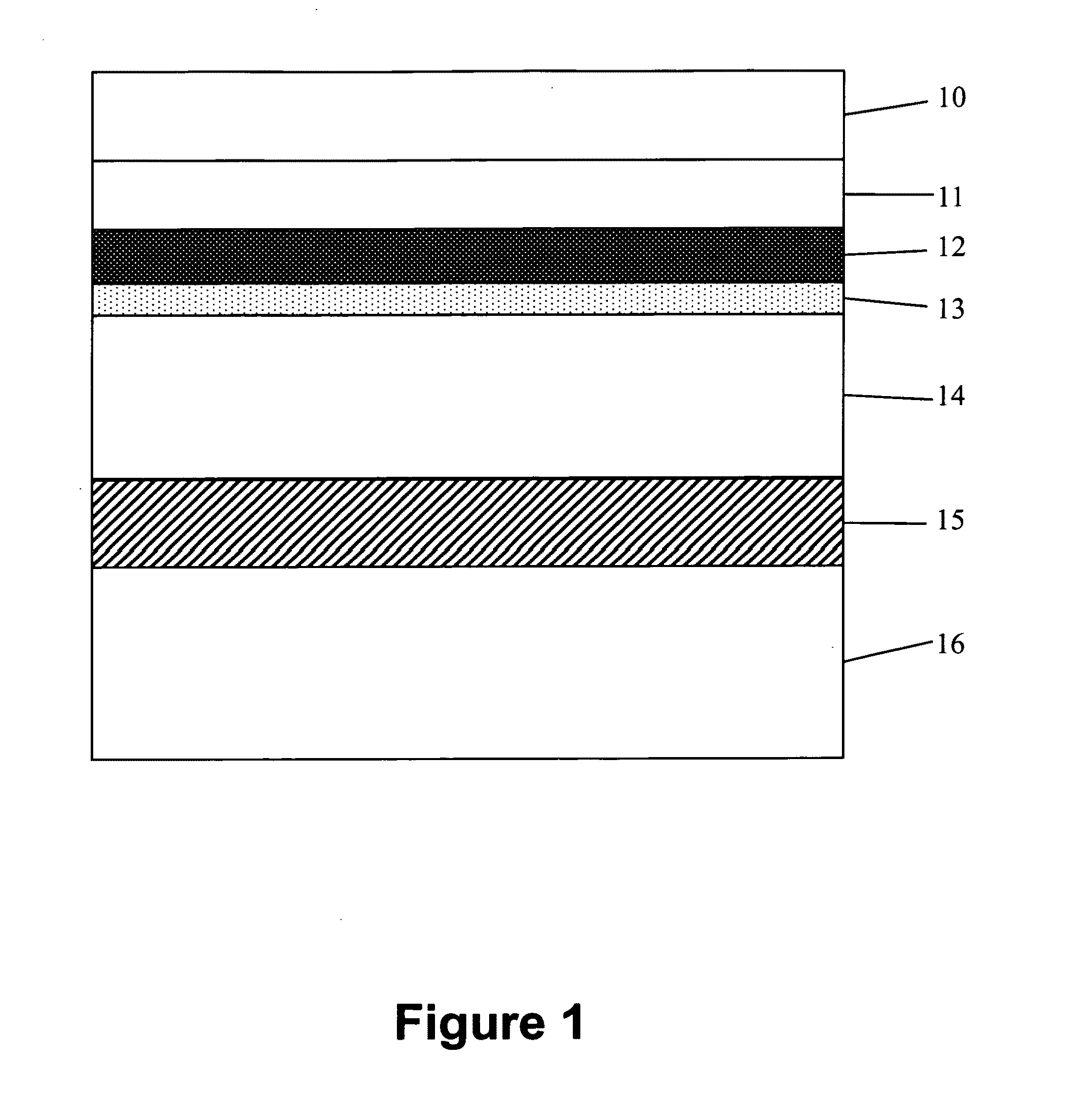
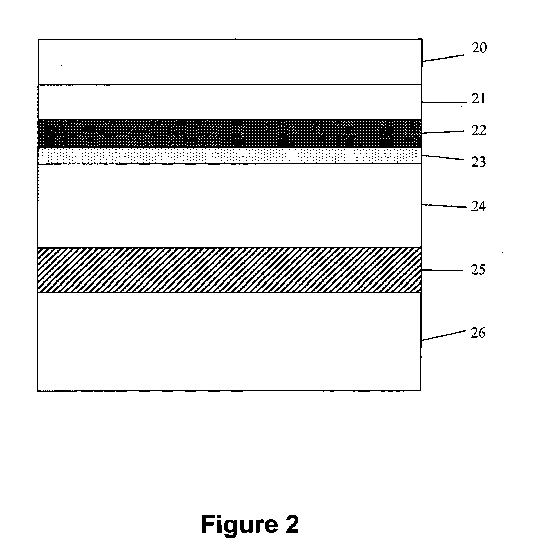
[0039]Referring to FIG. 1, there is shown a sectional view of a conventional prior art CIGS solar cell comprising a buffer layer deposited through a Chemical Bat...


PUM


Abstract

A method to manufacture Copper Indium Gallium di Selenide (Cu(In,Ga)Se2) thin film solar cell includes evaporating elemental Cu, In, Ga, and Se flux sources onto a heated substrate in a single vacuum system to form a non-intentionally doped Cu(In,Ga)Se2 p-type conductivity layer and exposing the p-type conductivity layer to a thermally evaporated flux of Beryllium (Be) atoms to convert a surface layer of the p-type conductivity layer to an n-type conductivity layer resulting in a buried Cu(In,Ga)Se2 p-n homojunction. Also, the source of Be atoms includes a circular rod of Be having a uniform cross-section that is resistively heated and having its temperature controlled by passing an electrical current through the rod.

Description

FIELD OF THE INVENTION[0001]This invention relates to the field of thin-film solar cells and, more particularly, to a manufacturing method and apparatus for a copper indium gallium diselenide (Cu (In, Ga)Se2) solar cell using a continuous in-vacuo deposition of semiconductor material forming the p-n junction and buffer layers.BACKGROUND OF THE INVENTION[0002]The search for renewable energy sources that provide a long term and sustainable energy source for future generations of mankind while mitigating global warming trends associated with the burning of fossil fuels has received worldwide attention. One such renewable energy source, which may compete with current non-renewable energy sources is a solar cell. Solar cell usage is expected to grow substantially as the cost to manufacture solar cells decreases to a point where it may economically compete with current non-renewable energy sources. Thin film semiconductor deposition technology used in solar cell production has increased r...

Claims


Application Information

Patent Timeline
IPC IPC(8): H01L31/0264H01L21/06
CPCH01L21/02568H01L21/02579H01L21/02664Y02E10/547H01L31/0323H01L31/068Y02E10/541H01L31/0322Y02P70/50
Inventor MALIK, ROGER J.
Owner RJM SEMICON
Why Eureka
Try Eureka