Semiconductor device and method for manufacturing the same

a semiconductor and device technology, applied in semiconductor devices, digital storage, instruments, etc., to achieve the effect of improving the reliability of the semiconductor devi

Inactive Publication Date: 2011-12-08
HITACHI LTD
View PDF1 Cites 44 Cited by
  • Summary
  • Abstract
  • Description
  • Claims
  • Application Information

AI Technical Summary

Benefits of technology

[0032]According to the invention, the reliability of the semiconductor device can be improved.

Problems solved by technology

While the laser annealing can perform a heat treatment at a high temperature in a short time, there may be a problem that a laser transmitting a layer to be subjected to the heat treatment may heat a heat feasible device at the lower layer thereby causing damages.

Method used


Image

  • Semiconductor device and method for manufacturing the same
  • Semiconductor device and method for manufacturing the same
  • Semiconductor device and method for manufacturing the same

Examples


first embodiment

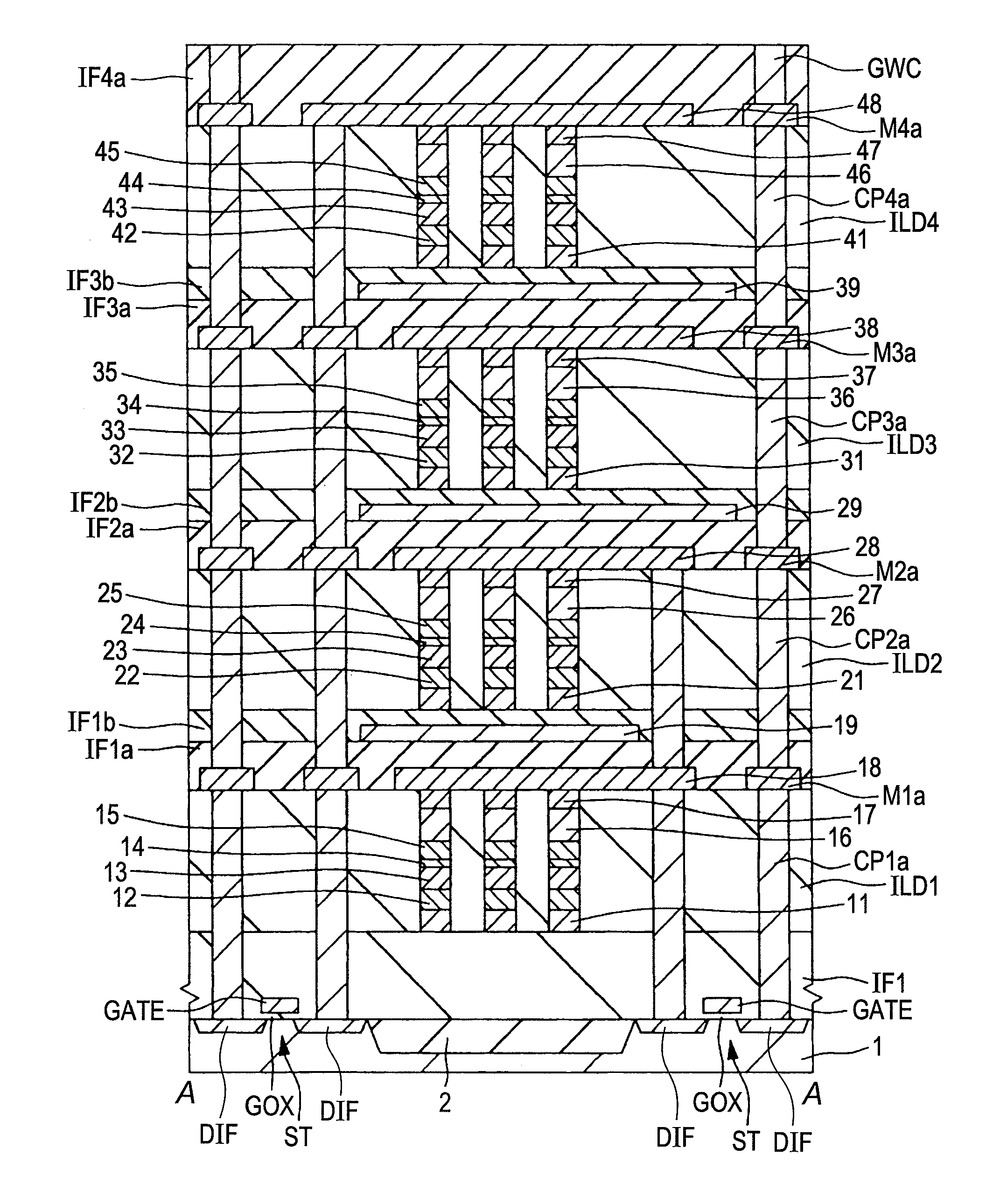
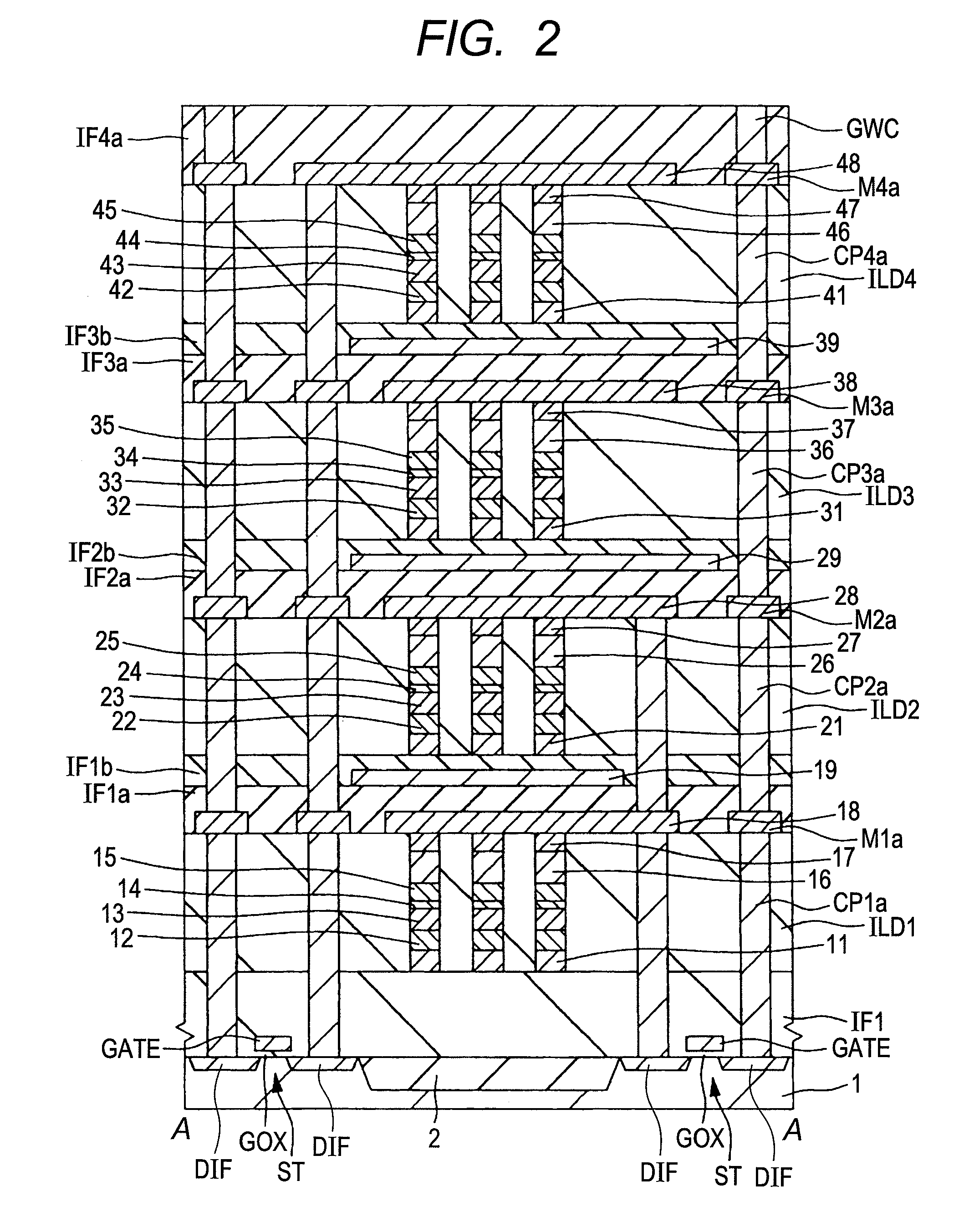
[0085]In this embodiment, description is to be made to a semiconductor device having a cross-point-type memory matrix where multiple self-aligned memory cells are formed in perpendicular to intersections between bit lines and word lines, having a diode as a selection device, and having a phase-change memory as a storage device.

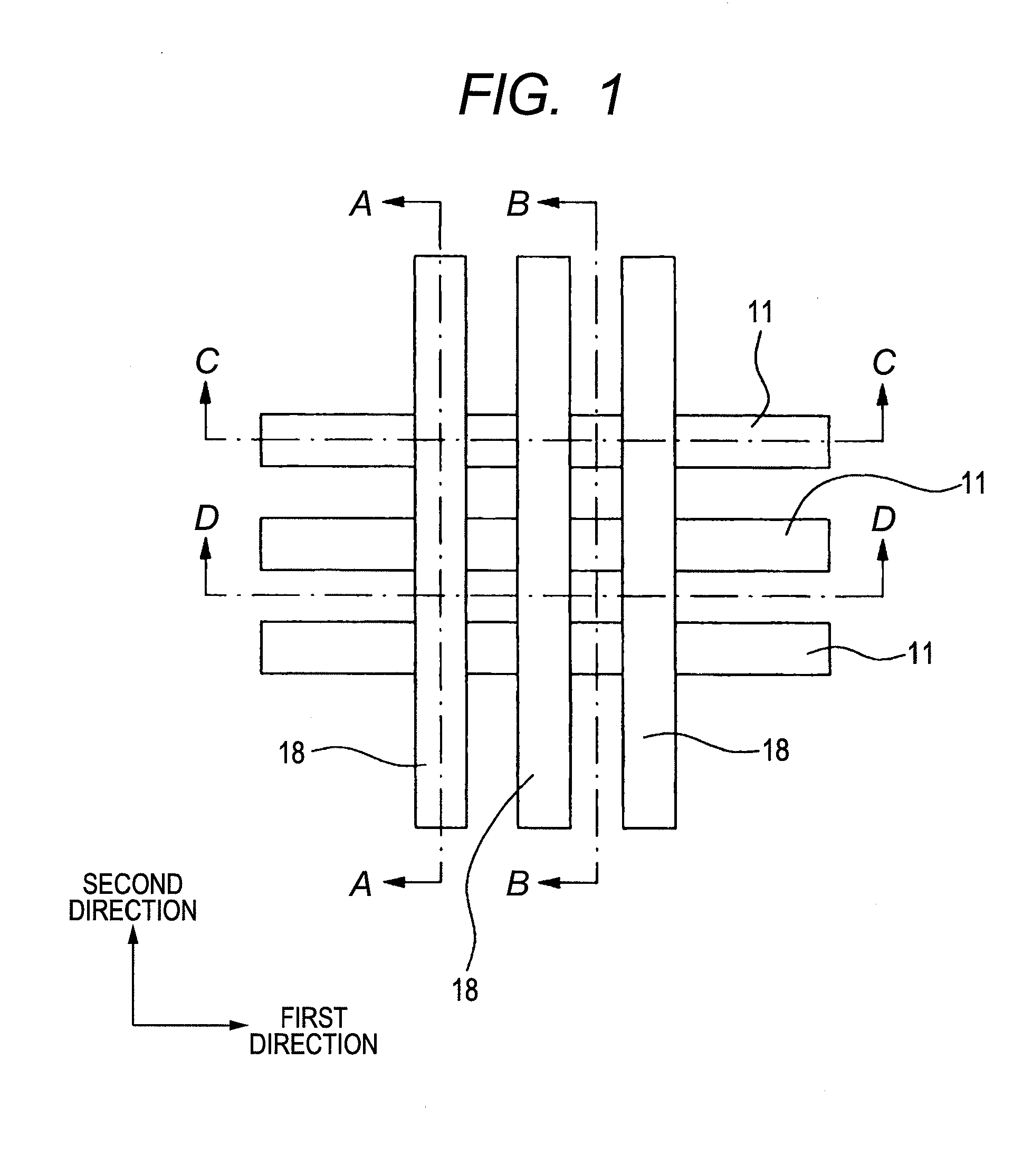
[0086]At first, FIG. 1 to FIG. 6 show a portion of a cross sectional view of a phase-change memory in this embodiment. FIG. 1 is a plan view of a phase-change memory of this embodiment and shows a structure in which multiple bit lines 18 extending in a stripe shape in a second direction perpendicular to a first direction are formed in a layer above multiple word lines 11 extending in a stripe shape in the first direction. In FIG. 1, only the word lines 11 and the bit liens 18 are shown for easy understanding of the drawing. FIG. 2, FIG. 3, FIG. 4, and FIG. 5 are cross sectional views for main portions along lines A-A, B-B, C-C, and D-D in FIG. 1. FIG. 6 is a p...

second embodiment

[0148]In the first embodiment, a semiconductor device having a cross-point-type phase-change memory has been described. In this embodiment, a structure of a semiconductor device having a vertical chain memory type phase-change memory is to be described with reference to FIG. 23 to FIG. 40.

[0149]At first, a structure of a phase-change memory of this embodiment is to be described with reference to FIG. 23 to FIG. 25. FIG. 23 shows a plan view of a phase-change memory, FIG. 24 shows a cross sectional view for a main portion along line E-E in FIG. 23, and FIG. 25 shows a cross sectional view for a main portion along line F-F in FIG. 23. In FIG. 25, however, structures in the layer above a metal interconnect M1 shown in FIG. 24 is not illustrated. FIG. 23 is a plan view showing the upper surface of an insulating film 56 and the structure above the insulating film 56 is shown by a broken line only for the contours of metal interconnects M1 and interconnects ML1 to ML4.

[0150]As shown in FI...

third embodiment

[0195]In this embodiment, description is to be made to a semiconductor device having a logic circuit including CMISFET. FIG. 41 shows a semiconductor device of this embodiment. As shown in FIG. 41, CMISFET of this embodiment (hereinafter simply referred to as CMISFET) has a structure in which multiple CMISs are stacked over a semiconductor substrate 1. Multiple device isolation regions 3 are formed in the upper surface of the semiconductor substrate 1, and a p-well 4a or an n-well 4b is formed in the upper surface of the semiconductor substrate 1 between the device isolation regions 3. A gate electrode GATE is formed over the p-well 4a and over the n-well 4b respectively by way of a gate insulating film GOX, and a side wall SW is formed on the side wall of the gate electrode GATE. The side wall SW is an insulating film comprised of, for example, silicon oxide, silicon nitride, or a stacked film thereof, and extension regions 5a, 5b are formed to the respective upper surfaces of the ...


PUM


Abstract

A technique used for a semiconductor device formed by stacking multiple structural bodies each having a semiconductor device, for preventing generation of thermal load on a structural body at a lower layer which is caused by a laser used in a step of forming a structural body at an upper layer. In a phase-change memory including multiple stacked memory matrices, a metal film is disposed between a memory matrix at a lower layer and a memory matrix at an upper layer formed over the memory matrix at the lower layer, in which the laser used for forming the memory matrix is reflected at the metal film and prevented from transmitting the metal film, thereby preventing the phase-change material layer, etc. in the memory matrix at the lower layer from being directly heated excessively by the laser.

Description

CLAIM OF PRIORITY[0001]The present application claims priority from Japanese patent application JP 2010-126983 filed on Jun. 2, 2010, the content of which is hereby incorporated by reference into this application.FIELD OF THE INVENTION[0002]The present invention relates to a semiconductor device and a method for manufacturing the same and particularly to a semiconductor device having a structure of stacking layers each containing a semiconductor device as well as a technique which is effectively applied to the manufacture of the semiconductor device.BACKGROUND OF THE INVENTION[0003]In recent years, in the manufacturing process of semiconductor device having a logic circuit or a non-volatile memory, a heating system using a laser has been used frequently instead of a heating system such as a lamp system used so far when heating the semiconductor device during a manufacturing process. Since laser annealing can apply a heat treatment at a high temperature in a short time and can preven...

Claims


Application Information

Patent Timeline
Patent Type & Authority Applications(United States)
IPC IPC(8): H01L47/00
CPCH01L27/2409H01L27/2454H01L27/2481H01L45/1683H01L45/1233H01L45/144H01L45/1675H01L45/06H10B63/34H10B63/84H10B63/20H10N70/231H10N70/826H10N70/8828H10N70/066H10N70/063
Inventor SHIMA, AKIOSASAGO, YOSHITSKAMINE, TOSHIYUKIKINOSHITA, MASAHARU
Owner HITACHI LTD
Why Eureka
Try Eureka