Semiconductor device

a technology of semiconductor devices and semiconductors, applied in semiconductor devices, solid-state devices, instruments, etc., can solve the problems of increased cost per storage capacity, difficulty in sufficiently reducing power consumption, and loss of stored data, so as to achieve the effect of increasing the degree of integration and reducing the layout area

Inactive Publication Date: 2011-12-08
SEMICON ENERGY LAB CO LTD
View PDF0 Cites 38 Cited by
  • Summary
  • Abstract
  • Description
  • Claims
  • Application Information

AI Technical Summary

Benefits of technology

[0028]Further, in an embodiment of the present invention, a surface of a gate electrode of a transistor in a lower portion (a transistor including a material other than an oxide semiconductor) and a source electrode of a transistor in an upper portion (a transistor including an oxide semiconductor) which is provided on and in contact with the gate electrode are formed by using materials with which the source electrode has etching se

Problems solved by technology

For that reason, another writing operation (refresh operation) is necessary at predetermined intervals, and it is difficult to sufficiently reduce power consumption.
Furthermore, since stored data is lost when power is not supplied, an additional storage device using a magnetic material or an optical material is needed in order to hold data for a long time.
However, cost per storage capacity is increased because a circuit such as a flip-flop is used.
Moreover, as in a DRAM, stored data in an SRAM is lost when power is not supplied.
However, a gate insulating la

Method used


Image

  • Semiconductor device
  • Semiconductor device
  • Semiconductor device

Examples


embodiment 1

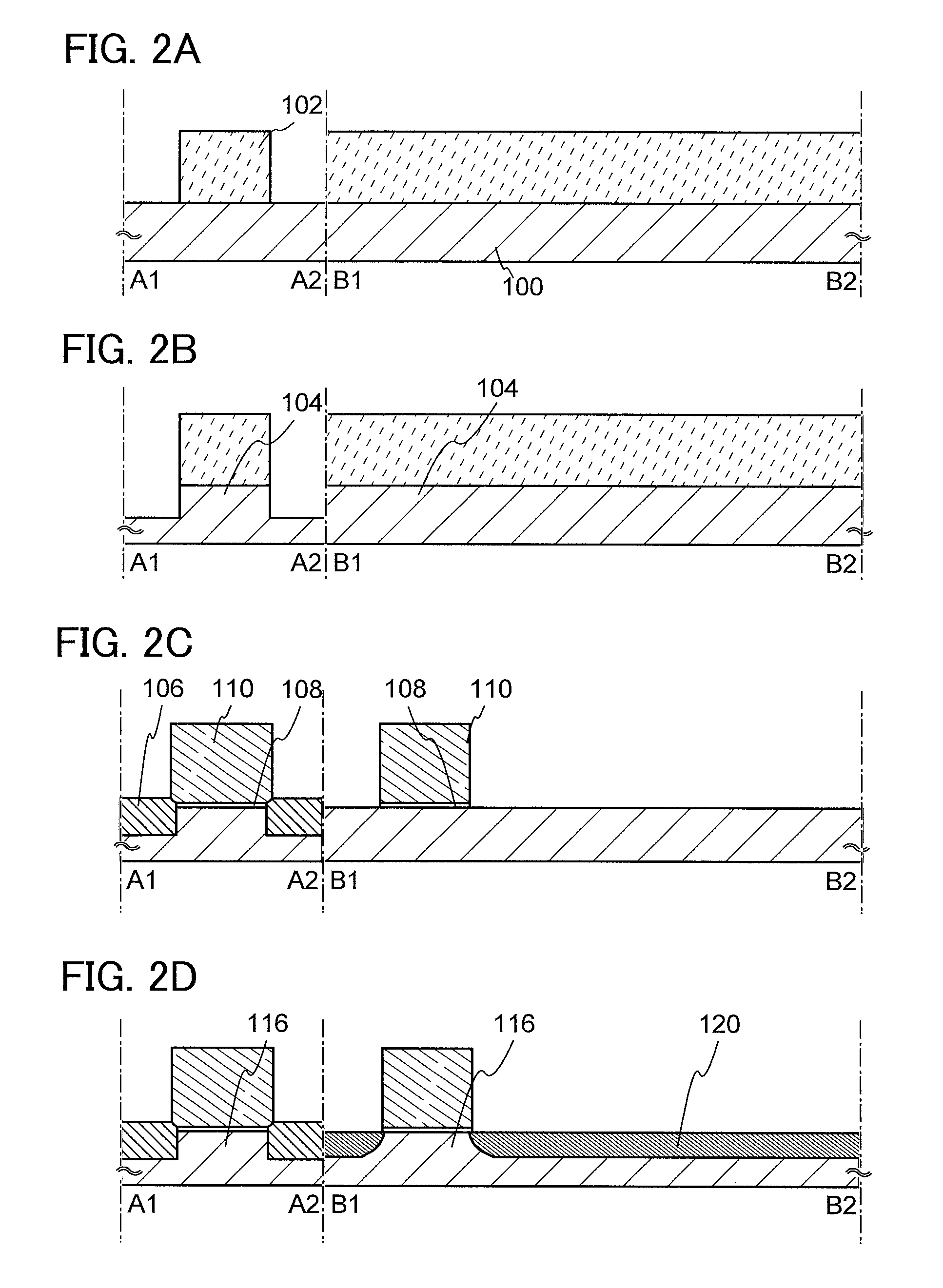
[0048]In this embodiment, a structure of a semiconductor device according to an embodiment of the present invention and a method for manufacturing the semiconductor device will be described with reference to FIGS. 1A and 1B, FIGS. 2A to 2D, FIGS. 3A to 3D, FIGS. 4A to 4C, and FIGS. 5A to 5C.

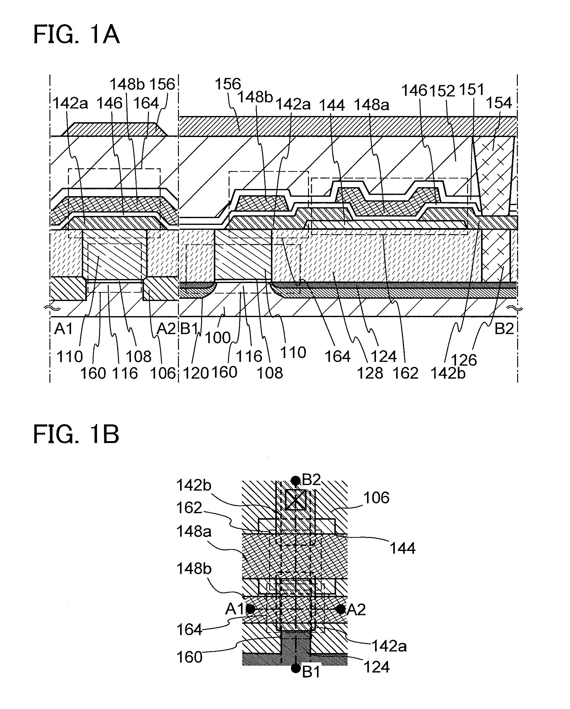
[0049]FIGS. 1A and 1B illustrate an example of a structure of a semiconductor device. FIG. 1A is a cross-sectional view of the semiconductor device, and FIG. 1B is a plan view of the semiconductor device. Here, FIG. 1A corresponds to a cross section along line A1-A2 and line B1-B2 in FIG. 1B. The semiconductor device illustrated in FIGS. 1A and 1B includes a transistor 160 including a first semiconductor material in a lower portion, and a transistor 162 including a second semiconductor material in an upper portion. Here, the first semiconductor material is preferably different from the second semiconductor material. For example, a semiconductor material other than an oxide semiconductor can be us...

embodiment 2

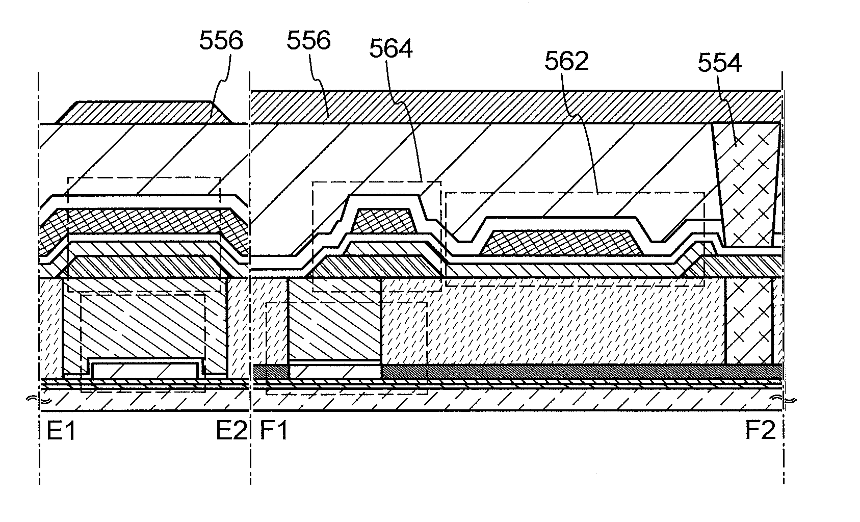
[0139]In this embodiment, a structure of a semiconductor device according to another embodiment of the invention disclosed herein and a method for manufacturing the semiconductor device will be described with reference to FIGS. 6A and 6B, FIGS. 7A to 7H, FIGS. 8A to 8E, FIGS. 9A to 9C, and FIGS. 10A to 10C.

[0140]FIGS. 6A and 6B illustrate an example of a structure of a semiconductor device according to this embodiment. FIG. 6A is a cross-sectional view of the semiconductor device, and FIG. 6B is a plan view of the semiconductor device. Here, FIG. 6A illustrates a cross section taken along line E1-E2 and line F1-F2 in FIG. 6B. The semiconductor device illustrated in FIGS. 6A and 6B includes a transistor 560 including a first semiconductor material in a lower portion and a transistor 562 including a second semiconductor material in an upper portion. Here, the first semiconductor material is preferably different from the second semiconductor material. For example, the first semiconduct...

embodiment 3

[0220]In this embodiment, a circuit configuration and operation of a semiconductor device according to an embodiment of the invention disclosed herein will be described with reference to FIGS. 11A-1 to 11B. In the description of circuit diagrams in FIGS. 11A-1 to 11B, reference numerals are the same as those in the semiconductor device in FIGS. 1A and 1B. Note that in each of the circuit diagrams, “OS” may be written beside a transistor in order to indicate that the transistor includes an oxide semiconductor.

[0221]In the semiconductor device illustrated in FIG. 11A-1, a first wiring (a 1st line) and a source electrode of a transistor 160 are electrically connected to each other. A second wiring (a 2nd line) and a drain electrode of the transistor 160 are electrically connected to each other. A third wiring (a 3rd line) and one of a source electrode and a drain electrode of a transistor 162 are electrically connected to each other, and a fourth wiring (a 4th line) and a gate electrod...


PUM


Abstract

It is an object to provide a semiconductor device with a novel structure in which stored data can be held even when power is not supplied and there is no limitation on the number of writings. A semiconductor device includes a second transistor and a capacitor provided over a first transistor. A source electrode of the second transistor which is in contact with a gate electrode of the first transistor is formed using a material having etching selectivity with respect to the gate electrode. By forming the source electrode of the second transistor using a material having etching selectivity with respect to the gate electrode of the first transistor, a margin in layout can be reduced, so that the degree of integration of the semiconductor device can be increased.

Description

BACKGROUND OF THE INVENTION[0001]1. Field of the Invention[0002]An embodiment of the invention disclosed herein relates to a semiconductor device using a semiconductor element and a method for manufacturing the semiconductor device.[0003]2. Description of the Related Art[0004]Storage devices using semiconductor elements are broadly classified into two kinds of devices: a volatile device that loses stored data when power is not supplied, and a non-volatile device that holds stored data even when power is not supplied.[0005]A typical example of a volatile storage device is a dynamic random access memory (DRAM). A DRAM stores data in such a manner that a transistor included in a storage element is selected and charge is stored in a capacitor.[0006]When data is read from a DRAM, charge in a capacitor is lost from the above-described principle; thus, another writing operation is necessary whenever data is read. Moreover, a transistor included in a storage element has a leakage current (o...

Claims


Application Information

Patent Timeline
IPC IPC(8): H01L27/108H01L27/088H01L21/336
CPCG11C16/0433H01L27/11521H01L27/10852H01L27/1225H01L27/1156H10B41/70H10B41/30H10B99/00H10B12/00H10B12/033
Inventor ISOBE, ATSUOIEDA, YOSHINORIKATO, KIYOSHIYAKUBO, YUTOHATA, YUKI
Owner SEMICON ENERGY LAB CO LTD
Why Eureka
Try Eureka