Micromechanical Component

a micromechanical and component technology, applied in the direction of fixed microstructure devices, semiconductor/solid-state device details, semiconductor devices, etc., can solve the problems of microstructure production, thickness variation, wave or wave, etc., and achieve low cost, low degree of complexity, and reliable removal

Active Publication Date: 2011-12-08
ROBERT BOSCH GMBH
View PDF1 Cites 10 Cited by
  • Summary
  • Abstract
  • Description
  • Claims
  • Application Information

AI Technical Summary

Benefits of technology

[0011]The step of removing the bonding material may be implemented, for example, using a polishing process. By this means, the bonding material outside of the trench structure may be reliably removed.
[0012]In an alternative embodiment, after depositing the layer of bonding material, an additional filling material is introduced into a recess of the layer of the bonding material. The removal of the bonding material outside of the trench structure is carried out, using an etching process in which the bonding material and the additional filling material exhibit essentially the same etching rate. This procedure is associated with relatively low costs.
[0013]In a further exemplary embodiment, the first substrate is provided with...

Problems solved by technology

However, the “topography” associated with the connecting structure or “material plane” projecting from the upper surface of the functional substrate has an adverse influence on the production of the microstructure, during which a photolithographic patterning method is used.
A result of the presence of the connecting structure situated about the subsequent microstructure is that in this region, the photoresist used in the patterning method ...

Method used


Image

  • Micromechanical Component
  • Micromechanical Component
  • Micromechanical Component

Examples


Embodiment Construction

[0036]With the aid of the following figures, methods for manufacturing a micromechanical component are described in which two substrates are joined to one another within the scope of a wafer bonding process. Processes and materials customary in semiconductor and microsystems technology may be used in the manufacturing methods, which means that these will only be discussed in part. Moreover, it is emphasized that further processes may be carried out in addition to the method steps shown and described.

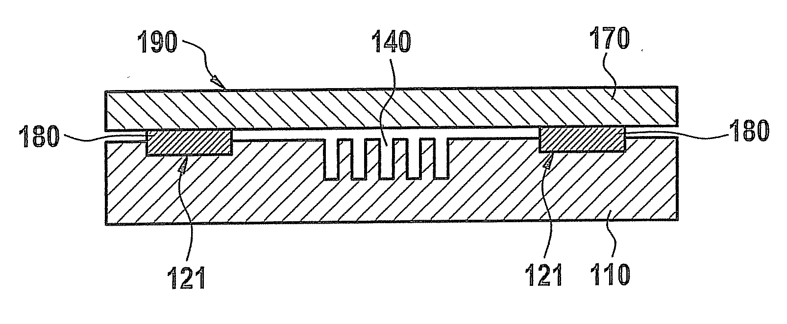
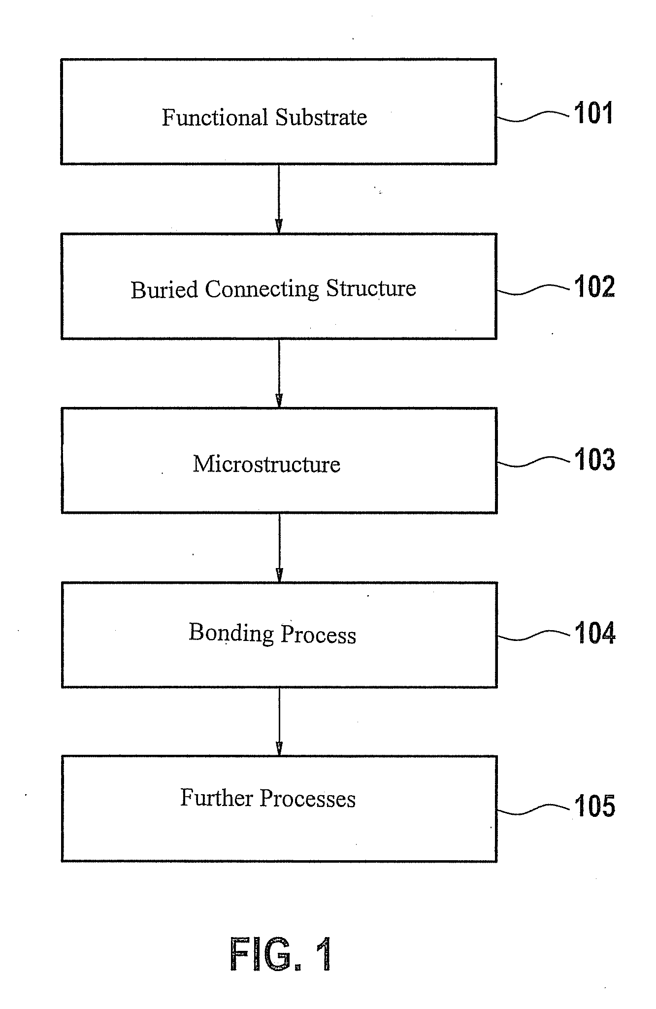
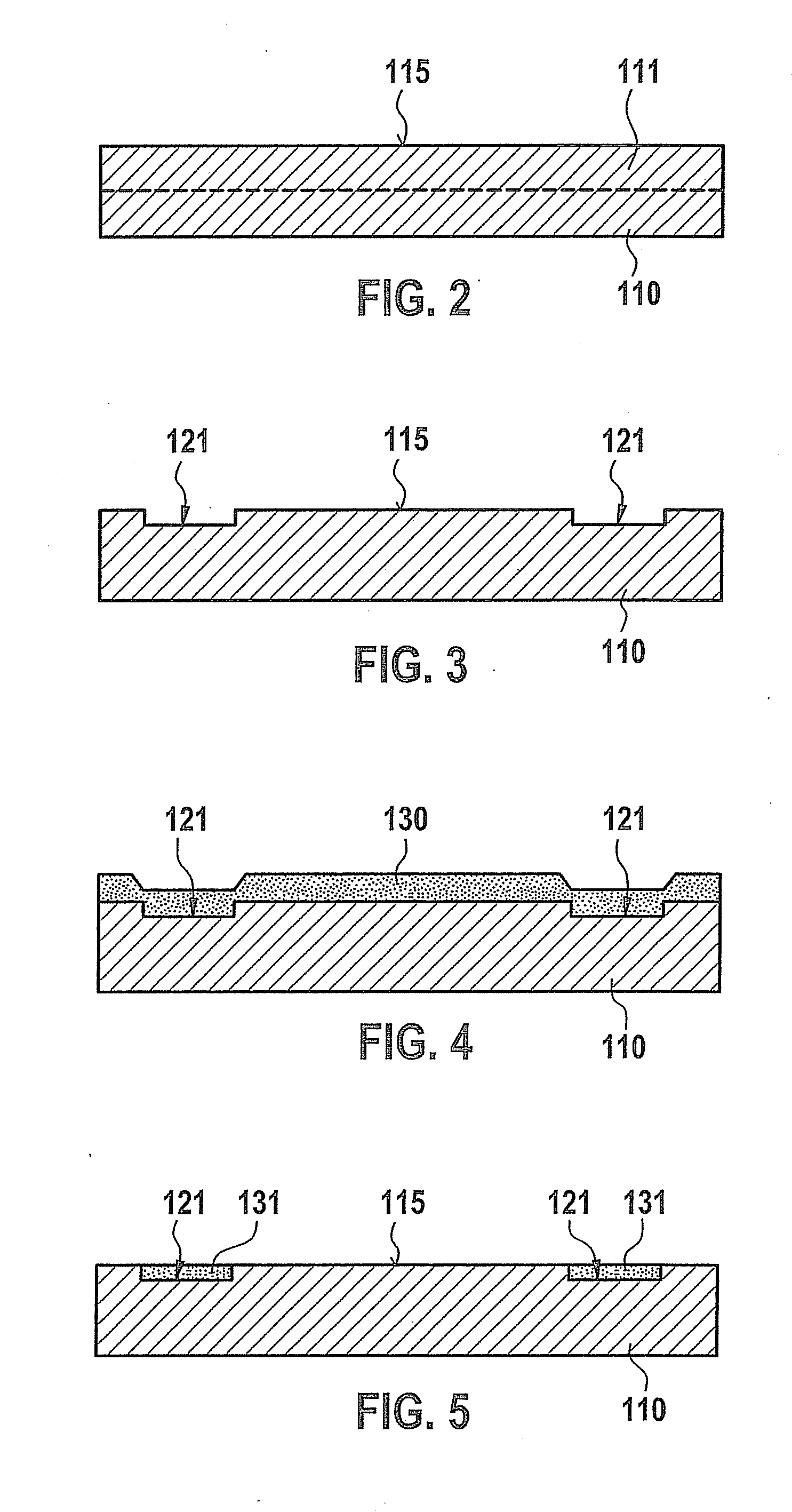
[0037]FIG. 1 shows a flow chart of a method for manufacturing a micromechanical component, which may be, e.g., an inertial sensor. In the method, a first substrate, which has a functional layer on one side, and which is referred to hereinafter as a functional substrate, is prepared in a step 101. In a subsequent step 102, a buried, frame-shaped connecting structure, also referred to as a “bonding layer” or “bonding frame,” which extends to an upper surface of the substrate (or of the fun...


PUM


Abstract

A method is described for manufacturing a micromechanical component. The method includes providing a first substrate, forming a first connecting structure on the first substrate, and forming a microstructure on the first substrate after forming the first connecting structure. The microstructure has at least one movable functional element. The method further includes providing a second substrate having a second connecting structure, and joining the first and second substrates by carrying out a bonding process, the first and second connecting structures being joined to form a common connecting structure, and a sealed cavity being formed in the region of the microstructure. The method provides that the first connecting structure takes the form of a buried connecting structure extending up to an upper surface of the first substrate. Also described is a related micromechanical component.

Description

RELATED APPLICATION INFORMATION[0001]The present application claims priority to and the benefit of German patent application no. 10 2010 029 709.7, which was filed in Germany on Jun. 4, 2010, the disclosure of which is incorporated herein by reference.FIELD OF THE INVENTION[0002]The present invention relates to a micromechanical component and a method for manufacturing a micromechanical component, a first and a second substrate being joined to one another by carrying out a bonding process.BACKGROUND INFORMATION[0003]Micromechanical components, which are used, for example, in the automotive field as inertial or pressure sensors, normally have a microstructure including movable functional elements. The microstructure is also designated as a MEMS structure (microelectromechanical system). During the operation of the sensors, a deflection of a functional element is detected, for instance, via a change in the electrical capacitance with respect to a fixed reference electrode.[0004]A curr...

Claims


Application Information

Patent Timeline
IPC IPC(8): H01L21/52H01L29/84
CPCB81B1/00B81C3/00B81C1/00B81B7/02B81C1/00269B81B2201/0235B81B2201/0242B81B2201/0264
Inventor MAYER, THOMAS
Owner ROBERT BOSCH GMBH
Why Eureka
Try Eureka