

Rolled Copper Foil or Electrolytic Copper Foil for Electronic Circuit, and Method of Forming Electronic Circuit using same
a technology of electrolytic copper foil and electronic circuit, which is applied in the direction of circuit masks, superimposed coating processes, transportation and packaging, etc., can solve the problems of generating heat, sagging, and affecting the effect of circuit width, so as to prevent short circuits and defects in circuit width, the effect of preventing sagging
- Summary
- Abstract
- Description
- Claims
- Application Information
AI Technical Summary
Benefits of technology
Problems solved by technology
Method used
Image

Examples
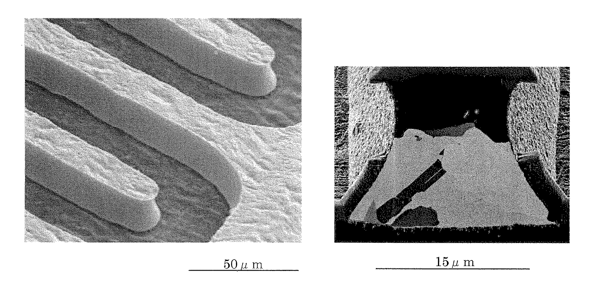
example 1
[0090]A rolled copper foil had a film thickness of 18 μm. The surface roughness Rz of this rolled copper foil was 0.7 μm. Platinum of 200 μg / dm2 was formed on this rolled copper foil in the foregoing platinum sputtering conditions.
[0091]And the copper foil was bonded to a resin substrate with the side opposite to the surface provided with the platinum layer as the adhesive surface.
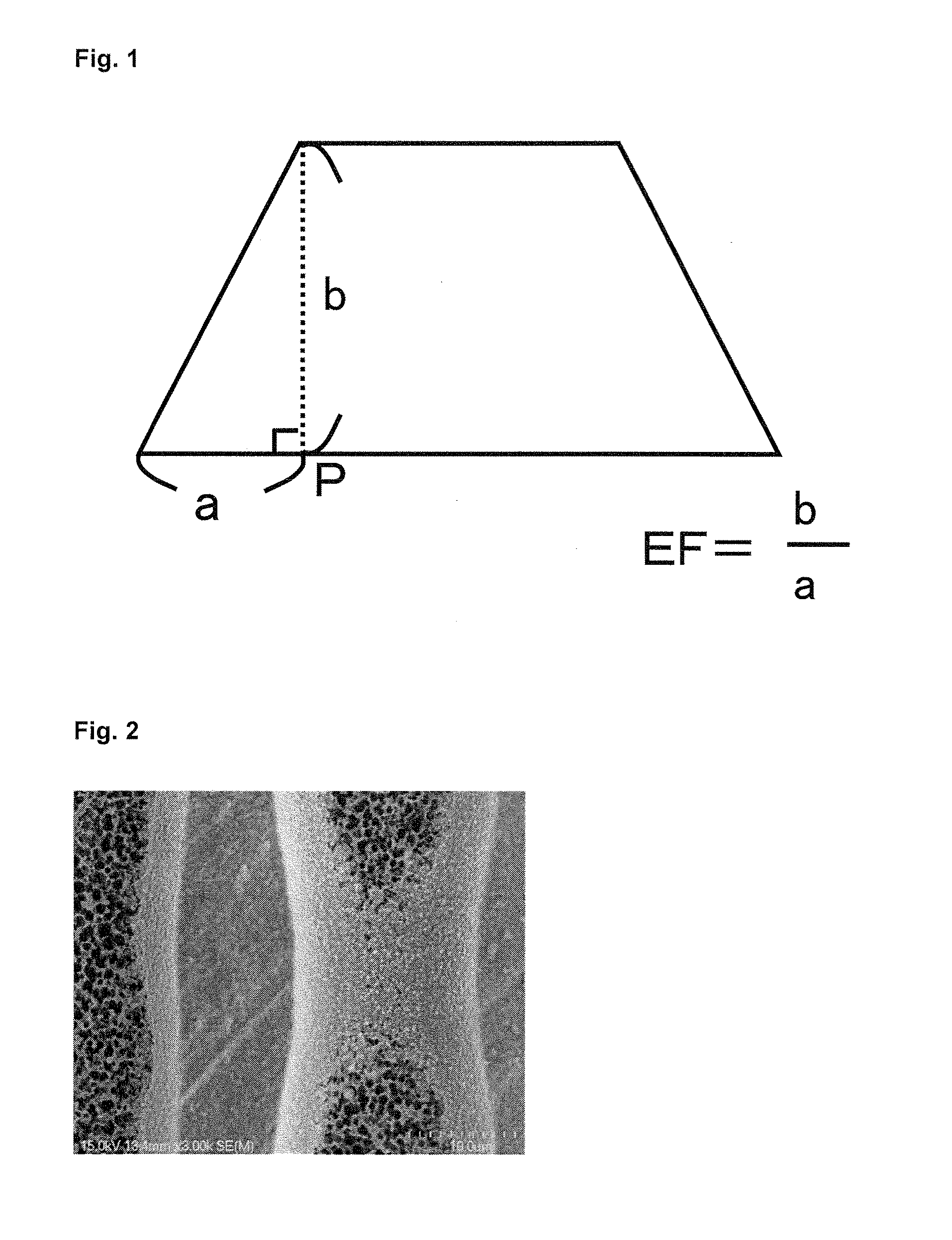
[0092]Subsequently, ten lines of a circuit were printed with the processes of resist application and exposure, and etching treatment was further performed to remove any unwanted part of the copper foil. The conditions of etching, circuit forming and measurement of the etching factor were as follows.
(Etching Conditions)
[0093]Aqueous ferric chloride solution: (37 wt %, Baum'e degree: 40°)
[0094]Solution temperature: 50° C.
[0095]Spray pressure: 0.15 MPa
(Circuit Forming Conditions)
[0096]Circuit pitch: There are two types of circuit pitches; namely, a 30 μm pitch and a 50 μm pitch, and the circuit pitch is chang...
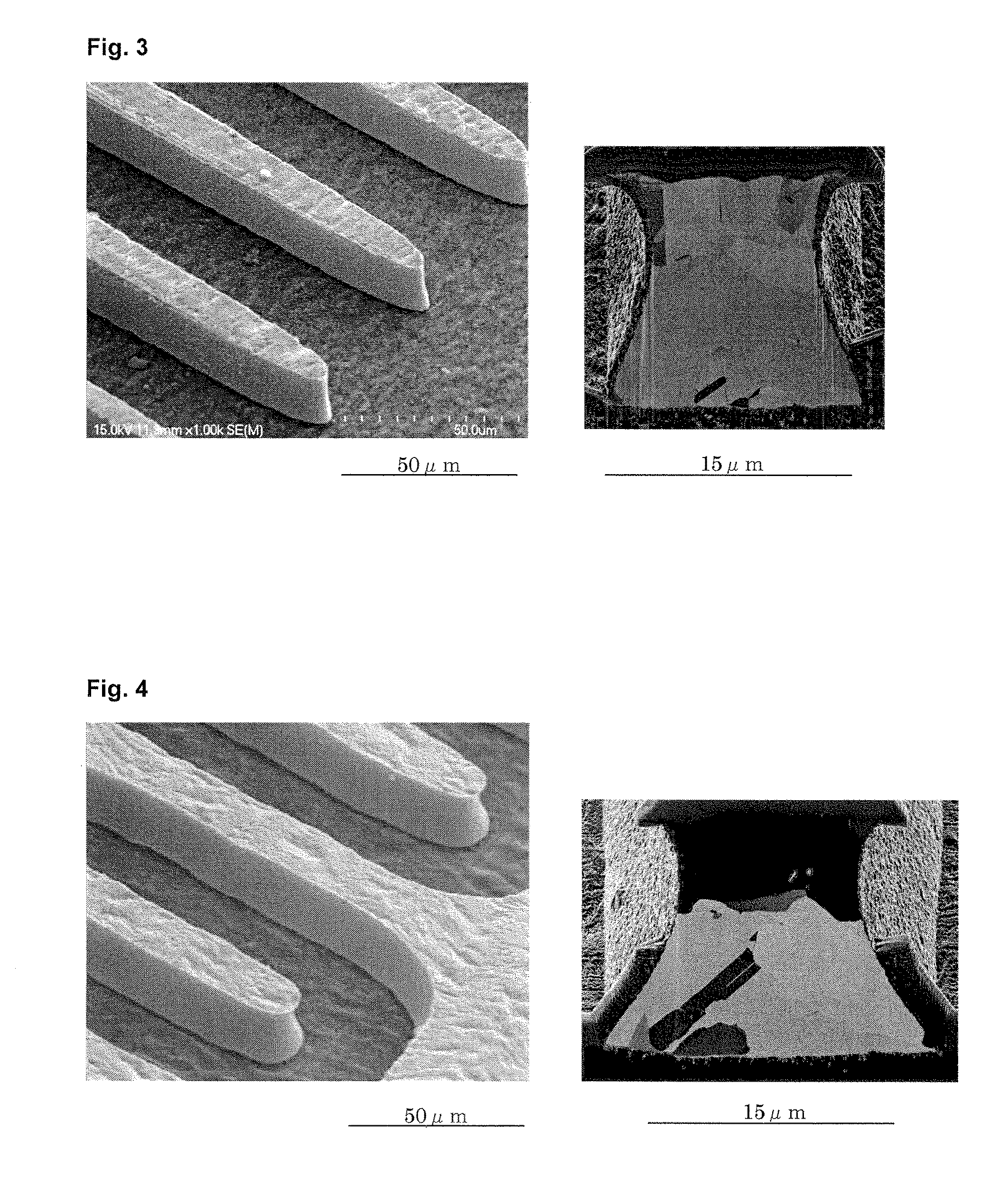
example 2
[0103]As with Example 1, a rolled copper foil had a film thickness of 18 μm. The surface roughness Rz of this rolled copper foil was 0.7 μm. Platinum of 500 μg / dm2 was formed on this rolled copper foil in the foregoing platinum sputtering conditions.
[0104]And the copper foil was bonded to a resin substrate with the side opposite to the surface provided with the platinum layer as the adhesive surface.
[0105]Subsequently, ten lines of a circuit were printed with the processes of resist application and exposure, and etching treatment was further performed to remove any unwanted part of the copper foil. The conditions of etching, circuit forming and measurement of the etching factor were as follows.
(Etching Conditions)
[0106]Aqueous ferric chloride solution: (37 wt %, Baum'e degree: 40°)
[0107]Solution temperature: 50° C.
[0108]Spray pressure: 0.15 MPa
(50 μm Pitch Circuit Formation)
[0109]Resist L / S=33 μm / 17 μm; finished circuit top (upper part) width: 15 μm; etching time: around 105 seconds...
example 3
[0113]In this Example, a rolled copper foil had a film thickness of 9 μm. The surface roughness Rz of this rolled copper foil was 0.7 μm. Platinum of 900 μg / dm2 was formed on this rolled copper foil in the foregoing platinum sputtering conditions.
[0114]And the copper foil was bonded to a resin substrate with the side opposite to the surface provided with the platinum layer as the adhesive surface.
[0115]Subsequently, ten lines of a circuit were printed with the processes of resist application and exposure, and etching treatment was further performed to remove any unwanted part of the copper foil. The conditions of etching, circuit forming and measurement of the etching factor were as follows.
(Etching Conditions)
[0116]Aqueous ferric chloride solution: (37 wt %, Baum'e degree: 40°)
[0117]Solution temperature: 50° C.
[0118]Spray pressure: 0.15 MPa
(30 μm Pitch Circuit Formation)
[0119]Since Example 3 used a copper foil having a thickness of 9 μm, the following conditions were used.
[0120]Res...
PUM
| Property | Measurement | Unit |
|---|---|---|
| angle | aaaaa | aaaaa |
| angle | aaaaa | aaaaa |
| inclined angle | aaaaa | aaaaa |
Abstract
Description
Claims
Application Information